GM393
LOW POWER DUAL DIFFERENTIAL COMPARATOR
Revision 1, May 2002 www.gammamicro.com
PRELIMINARY
1
The GM393 series consists of two independent precision voltage comparators with an offset voltage specification
as low as 2.0 mV max for two comparators which were designed specifically to operate from a single power supply
over a wide range of voltages. Operation from split power supplies is also possible and the low power supply
current drain is independent of the magnitude of the power supply voltage. These comparators also have a unique
characteristic in that the input common-mode voltage range includes ground, even though operated from a single
power supply voltage.
Application areas include limit comparators, simple analog to digital converters; pulse, squarewave and time
delay generators; wide range VCO; MOS clock timers; multivibrators and high voltage digital logic gates. The
GM393 series was designed to directly interface with TTL and CMOS. When operated from both plus and minus
power supplies, the GM393 series will directly interface with MOS logic where their low power drain is a distinct
advantage over standard comparators.
The GM393 is available in DIP-8 and SOP-8 packages.
Wide supply voltage range: ±1.0V to ±18V
Very low supply current drain (0.4 mA) -- independent of supply voltage
Low input biasing current: 25 nA
Low input offset current: ±5 nA
Maximum offset voltage: ±3 mV
Input common-mode voltage range includes ground
Differential input voltage range equal to the power supply voltage
Low output saturation voltage,: 250 mV at 4 mA
Output voltage compatible with TTL, DTL, ECL, MOS and CMOS logic systems
Advantages:
High precision comparators
Reduced V
OS
drift over temperature
Eliminates need for dual supplies
Allows sensing near GND
Compatible with all forms of logic
Power drain suitable for battery
operation
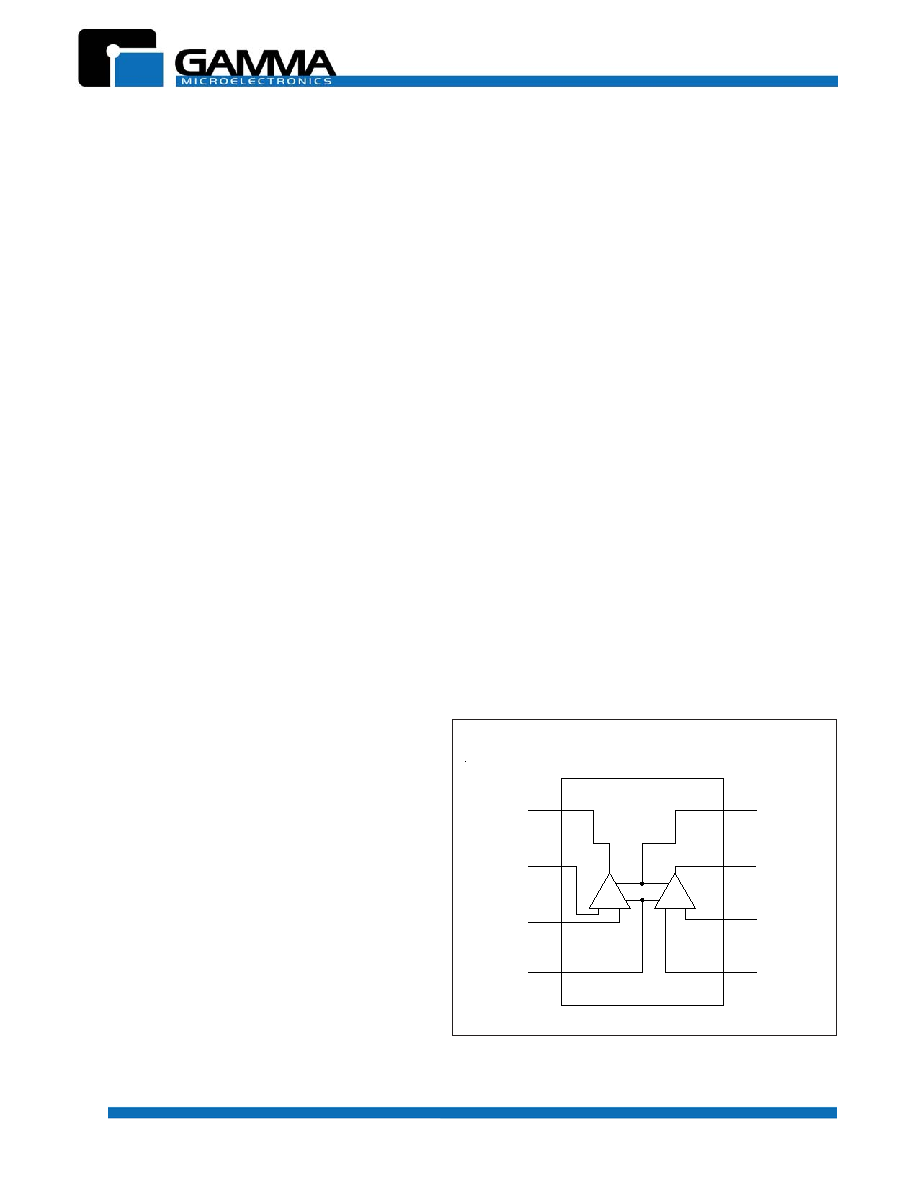
GND
4
3
2
1
-
-
+
+
A
B
OUTPUT A
OUTPUT B
INVERTING
INPUT A
NON-INVERTING
INPUT A
INVERTING
INPUT B
NON-INVERTING
INPUT B
5
6
7
8
V
CC
(Top View)
SOP8, DIP8 PACKAGE
CONNECTION DIAGRAM
GM393
LOW POWER DUAL DIFFERENTIAL COMPARATOR
Revision 1, May 2002 www.gammamicro.com
PRELIMINARY
2
R
E
T
E
M
A
R
A
P
L
O
B
M
Y
S
E
U
L
A
V
T
I
N
U
r
e
w
o
P
n
o
it
a
p
i
s
s
i
D
e
g
a
k
c
a
p
P
I
D
e
g
a
k
c
a
p
P
O
S
P
D
0
8
7
0
1
5
W
m
e
g
a
tl
o
V
y
l
p
p
u
S
V
C
C
6
3
V
t
n
e
r
r
u
C
t
u
p
n
I
I
O
0
5
A
m
e
g
n
a
R
e
r
u
t
a
r
e
p
m
e
T
g
n
it
a
r
e
p
O
T
J
0
7
+
o
t
0
C
∞
)
c
e
s
0
1
,
g
n
ir
e
d
l
o
S
(
e
r
u
t
a
r
e
p
m
e
T
d
a
e
L
T
D
A
E
L
0
6
2
C
∞
e
g
n
a
R
e
r
u
t
a
r
e
p
m
e
T
e
g
a
r
o
t
S
T
G
T
S
0
5
1
+
o
t
5
6
≠
C
∞
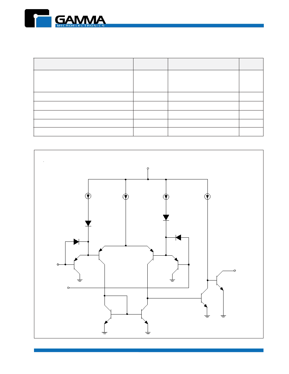
ABSOLUTE MAXIMUM RATINGS
V
CC
+ INPUT
OUTPUT
- INPUT
Q8
Q7
Q4
Q3
Q2
Q1
Q5
Q6
3.5
µ
A
3.5
µ
A
100
µ
A
100
µ
A
SCHEMATIC DIAGRAM
GM393
LOW POWER DUAL DIFFERENTIAL COMPARATOR
Revision 1, May 2002 www.gammamicro.com
PRELIMINARY
3
S
C
I
T
S
I
R
E
T
C
A
R
A
H
C
L
O
B
M
Y
S
S
N
O
I
T
I
D
N
O
C
T
S
E
T
N
I
M
P
Y
T
X
A
M
T
I
N
U
e
g
a
tl
o
V
t
e
s
ff
O
t
u
p
n
I
V
O
I
V
C
C
V
0
3
o
t
V
5
=
V
C
I
V
=
R
C
I
,
n
i
m
V
O
V
4
.
1
=
C
∞
5
2
2
5
V
m
e
g
n
a
r
ll
u
F
9
t
n
e
r
r
u
C
t
e
s
ff
O
t
u
p
n
I
I
O
I
V
O
V
4
.
1
=
C
∞
5
2
5
0
5
A
n
e
g
n
a
r
ll
u
F
0
5
1
t
n
e
r
r
u
C
s
a
i
B
t
u
p
n
I
I
S
A
I
B
V
O
V
4
.
1
=
C
∞
5
2
5
2
-
0
5
2
-
A
n
e
g
n
a
r
ll
u
F
0
0
4
-
e
g
a
tl
o
V
t
u
p
n
I
e
d
o
M
-
n
o
m
m
o
C
*
*
e
g
n
a
R
V
R
C
I
C
∞
5
2
V
o
t
0
C
C
5
.
1
-
V
e
g
n
a
r
ll
u
F
V
o
t
0
C
C
2
-
e
g
a
tl
o
V
t
u
p
t
u
O
l
e
v
e
L
-
w
o
L
V
L
O
I
L
O
,
A
m
4
=
V
D
I
V
1
-
=
C
∞
5
2
0
5
1
0
0
4
V
m
e
g
n
a
r
ll
u
F
0
0
7
l
a
it
n
e
r
e
ff
i
D
l
a
n
g
i
S
-
e
g
r
a
L
n
o
it
a
c
if
il
p
m
A
e
g
a
tl
o
V
A
D
V
V
C
C
V
,
V
5
1
=
O
o
t
V
4
.
1
=
,
V
4
.
1
1
R
L
k
5
1
>
V
o
t
C
C
C
∞
5
2
0
5
0
0
2
V
m
/
V
t
n
e
r
r
u
C
t
u
p
t
u
O
l
e
v
e
L
-
h
g
i
H
I
H
O
V
H
O
V
,
V
5
=
D
I
V
1
=
C
∞
5
2
1
.
0
0
5
A
n
V
H
O
V
,
V
0
3
=
D
I
V
1
=
e
g
n
a
r
ll
u
F
1
µ
A
t
n
e
r
r
u
C
t
u
p
t
u
O
l
e
v
e
L
-
w
o
L
I
L
O
V
L
O
,
V
5
.
1
=
V
D
I
V
1
-
=
C
∞
5
2
6
A
m
t
n
e
r
r
u
C
y
l
p
p
u
S
I
C
C
R
L
=
V
,
C
C
V
5
=
C
∞
5
2
8
.
0
0
.
1
A
m
R
L
=
V
,
C
C
V
0
3
=
e
g
n
a
r
ll
u
F
5
.
2
ELECTRICAL CHARACTERISTICS
(V
CC
= 5V, at specified free-air temperature, unless otherwise specified )
* All characteristics are measured under open loop conditions with zero common-mode input voltage unless otherwise specified.
Full range is 0∞C to 70∞C.
** The voltage at either input or common-mode should not be allowed to go negative by more than 0.3V.
The upper end of the common-mode voltage range is Vcc - 1.5V, but either or both inputs can go to 30V without damage.
R
E
T
E
M
A
R
A
P
S
N
O
I
T
I
D
N
O
C
T
S
E
T
N
I
M
P
Y
T
X
A
M
T
I
N
U
e
m
i
T
e
s
n
o
p
s
e
R
R
L
V
5
o
t
d
e
t
c
e
n
n
o
c
k
1
.
5
h
g
u
o
r
h
t
C
L
)
1
e
t
o
N
(
*
F
p
5
1
=
h
ti
w
p
e
t
s
t
u
p
n
i
V
m
0
0
1
e
v
ir
d
r
e
v
o
V
m
5
3
.
1
µ
s
p
e
t
s
t
u
p
n
i
l
e
v
e
l-
L
T
T
3
.
0
SWITCHING CHARACTERISTICS
* C
L
includes probe and jig capacitance.
NOTE 1: The response time specified is the interval between the input step function and the instant when the output crosses 1.4V.
GM393
LOW POWER DUAL DIFFERENTIAL COMPARATOR
Revision 1, May 2002 www.gammamicro.com
PRELIMINARY
4
3
9
3
M
G
E
G
A
K
C
A
P
8
P
O
S
8
P
I
D
8
S
3
9
3
M
G
8
D
3
9
3
M
G
ORDERING INFORMATION
GM393
LOW POWER DUAL DIFFERENTIAL COMPARATOR
Revision 1, May 2002 www.gammamicro.com
PRELIMINARY
5
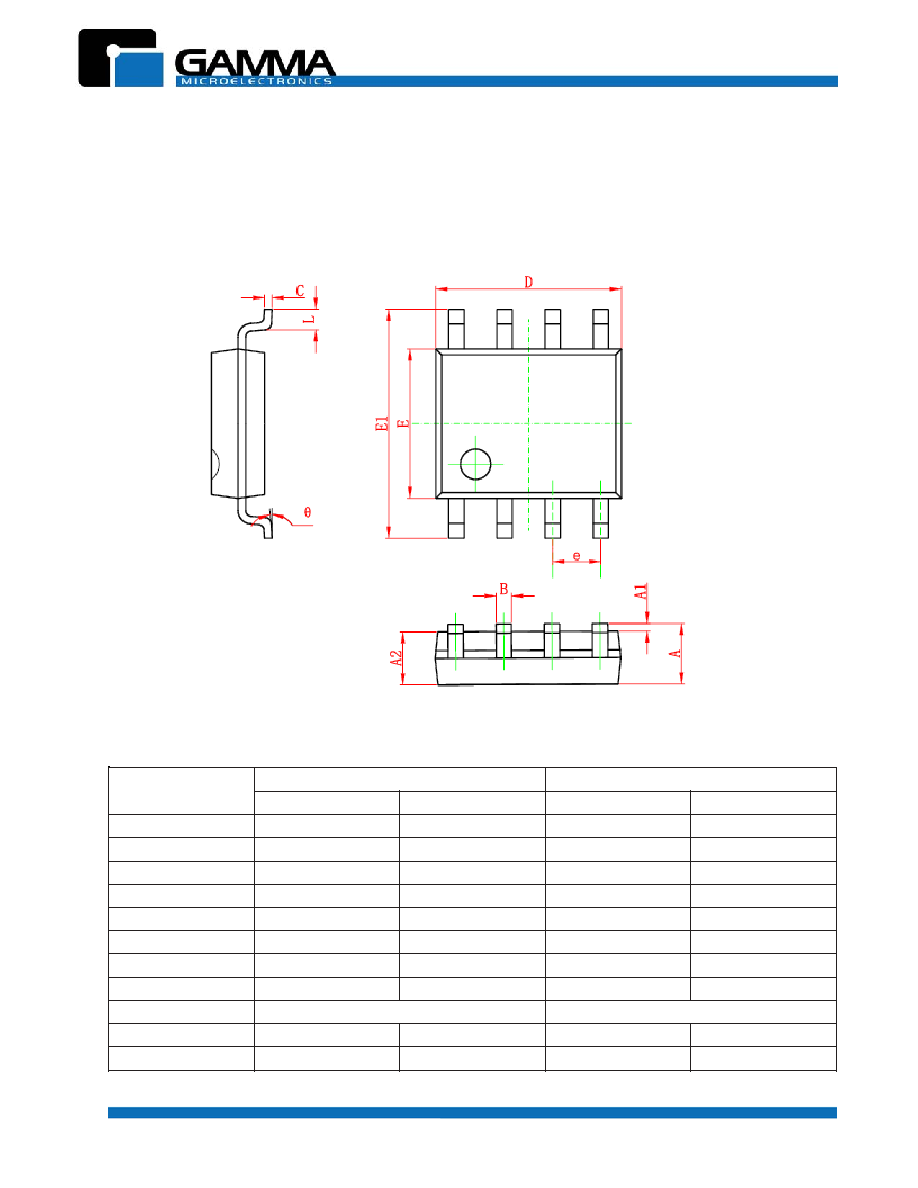
SOP-8 PACKAGE OUTLINE DIMENSIONS
L
O
B
M
Y
S
s
r
e
t
e
m
il
li
M
n
I
s
n
o
i
s
n
e
m
i
D
s
e
h
c
n
I
n
I
s
n
o
i
s
n
e
m
i
D
N
I
M
X
A
M
N
I
M
X
A
M
A
5
4
.
1
5
7
.
1
7
5
0
.
0
9
6
0
.
0
1
A
1
.
0
5
2
.
0
4
0
0
.
0
1
0
.
0
2
A
5
3
.
1
5
5
.
1
3
5
0
.
0
1
6
0
.
0
B
6
0
3
.
0
6
0
5
.
0
2
1
0
.
0
2
0
.
0
C
3
5
1
.
0
3
5
2
.
0
6
0
0
.
0
1
0
.
0
D
1
8
.
4
1
0
.
5
9
8
1
.
0
7
9
1
.
1
E
4
8
.
3
4
0
.
4
1
5
1
.
0
9
5
1
.
0
1
E
4
8
.
5
4
2
.
6
3
2
.
0
6
4
2
.
0
e
7
2
.
1
5
0
.
0
L
5
4
.
0
1
8
1
0
.
0
9
3
0
.
0
∞
0
∞
8
∞
0
∞
8