GM494
PULSE-WIDTH-MODULATION CONTROLLER
Revision 1, May 2002 www.gammamicro.com
PRELIMINARY
Complete PWM Power Control Circuit
Uncommitted outputs for 200mA sink or
source current
Internal protection against double pulse
at either output
Output control selects single-ended or
push-pull operation
Variable dead time control over
full range
Internal regulator provides stable 5V
reference supply with 5% tolerance
Design permits easy synchronization
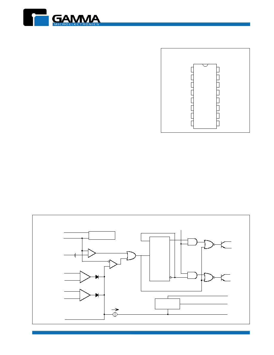
The GM494 is a comprises all the functions of a pulse-width-modulation (PWM) control circuit. Inteded mainly for
power-supply control, the GM494's verstility makes it easy to optimize the power-supply control circuit to your
specific application.
The GM494 includes two error amplifiers, an on-chip adjustable oscillator, a dead-time control (DTC) comparator,
a pulse-steering control flip-flop, a 5V, 5%-precision regulator, and output-control circuits. The error amplifiers
have a common-mode voltage range from ≠0.3 V to V
CC
≠ 2 V. The DTC comparator has a fixed offset, providing
~5% dead time. You can bypass the on-chip oscillator by terminating R
T
(pin 6) to the reference output and
providing a sawtooth input to C
T
(pin 5), or use the oscillator to drive the common circuits in synchronous multiple-
rail power supplies. You can assign the uncommitted output transistors to provide either common-emitter or
emitter-follower output. The GM494 allows either push-pull or single-ended output operation, which you select via
the output-control function. The design of the GM494 prevents either output from being pulsed twice during push-
pull operation.
PIN CONFIGURATIONS
FUNCTIONAL BLOCK DIAGRAM
1
1
2
3
4
5
6
7
8
16
15
14
13
12
11
10
9
2IN+
2IN-
REF
OUTPUT CTRL
C2
E2
E1
1IN+
1IN-
FEEDBACK
DTC
CT
RT
GND
C1
V
CC
Oscillator
6
5
RT
CT
0.1V
DTC
4
PWM
Comparator
Dead-Time
Control Comparator
1
2
Error Amplifier 1
1IN+
1IN-
1IN+
1IN-
16
15
Error Amplifier 2
+
-
+
-
3
FEEDBACK
0.7mA
GND
REF
V
CC
7
14
12
C1
8
E1
9
Q1
C2
E2
Q2
11
10
Pulse-Steering
Flip-Flop
>C1
1D
13
OUTPUT CONTROL
Reference
Regulator
GM494
PULSE-WIDTH-MODULATION CONTROLLER
Revision 1, May 2002 www.gammamicro.com
PRELIMINARY
2
R
E
T
E
M
A
R
A
P
L
O
B
M
Y
S
E
U
L
A
V
S
T
I
N
U
e
g
a
tl
o
V
y
l
p
p
u
S
V
C
C
1
4
V
e
g
a
tl
o
V
t
u
p
n
I
r
e
if
il
p
m
A
V
I
V
C
C
3
.
0
+
V
e
g
a
tl
o
V
t
u
p
t
u
O
r
o
t
c
e
ll
o
C
V
O
1
4
V
t
n
e
r
r
u
C
t
u
p
t
u
O
r
o
t
c
e
ll
o
C
I
O
0
5
2
A
m
e
g
n
a
R
e
r
u
t
a
r
e
p
m
e
T
r
i
A
-
e
e
r
F
g
n
it
a
r
e
p
O
T
A
0
7
+
o
t
0
C
∞
e
g
n
a
R
e
r
u
t
a
r
e
p
m
e
T
e
g
a
r
o
t
S
T
g
t
s
0
5
1
+
o
t
5
6
-
C
∞
)
.
c
e
s
0
1
r
o
f
e
s
a
c
m
o
r
f
m
m
6
.
1
(
e
r
u
t
a
r
e
p
m
e
T
d
a
e
L
T
L
0
6
2
C
∞
ABSOLUTE MAXIMUM RATINGS over operating free-air temperature range
(unless otherwise noted)
R
E
T
E
M
A
R
A
P
L
O
B
M
Y
S
N
I
M
X
A
M
S
T
I
N
U
e
g
a
tl
o
V
y
l
p
p
u
S
V
C
C
7
0
4
V
e
g
a
tl
o
V
t
u
p
n
I
r
e
if
il
p
m
A
V
I
3
.
0
-
V
C
C
2
-
V
e
g
a
tl
o
V
t
u
p
t
u
O
r
o
t
c
e
ll
o
C
V
O
-
0
4
V
)
r
o
t
s
i
s
n
a
r
T
h
c
a
E
(
t
n
e
r
r
u
C
t
u
p
t
u
O
r
o
t
c
e
ll
o
C
I
O
-
0
0
2
A
m
k
c
a
b
d
e
e
F
o
t
n
I
t
n
e
r
r
u
C
-
-
3
.
0
A
m
e
g
n
a
R
e
r
u
t
a
r
e
p
m
e
T
r
i
A
-
e
e
r
F
g
n
it
a
r
e
p
O
T
A
0
0
7
C
∞
y
c
n
e
u
q
e
r
F
r
o
t
a
ll
i
c
s
O
f
C
S
O
1
0
0
3
z
H
k
r
o
ti
c
a
p
a
C
g
n
i
m
i
T
C
T
7
4
.
0
0
0
0
0
1
F
n
r
o
t
s
i
s
e
R
g
n
i
m
i
T
R
T
8
.
1
0
0
5
k
RECOMMENDED OPERATING CONDITIONS
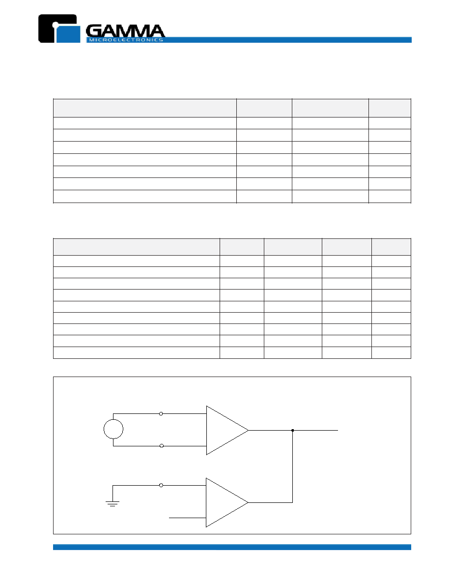
AMPLIFIER CHARACTERISTICS
V
I
+
-
+
-
V
REF
FEEDBACK
TERMINAL
AMPLIFIER
UNDER TEST
OTHER
AMPLIFIER
Figure 2

GM494
PULSE-WIDTH-MODULATION CONTROLLER
Revision 1, May 2002 www.gammamicro.com
PRELIMINARY
4
ABSOLUTE MAXIMUM RATINGS over operating free-air temperature range
V
CC
= 15V, f = 10kHz (unless otherwise noted)
R
E
T
E
M
A
R
A
P
*
S
N
O
I
T
I
D
N
O
C
T
S
E
T
N
I
M
*
*
P
Y
T
X
A
M
T
I
N
U
n
o
i
t
c
e
S
e
c
n
e
r
e
f
e
R
(
e
g
a
tl
o
V
t
u
p
t
u
O
V
F
E
R
)
I
O
A
m
1
=
5
7
.
4
5
5
2
.
5
V
n
o
it
a
l
u
g
e
R
t
u
p
n
I
V
C
C
V
0
4
o
t
V
7
=
-
2
5
2
V
m
n
o
it
a
l
u
g
e
R
t
u
p
t
u
O
I
O
A
m
0
1
o
t
A
m
1
=
-
1
5
1
V
m
e
r
u
t
a
r
e
p
m
e
T
h
ti
w
e
g
n
a
h
C
e
g
a
tl
o
V
t
u
p
t
u
O
T
A
X
A
M
o
t
N
I
M
=
-
2
.
0
1
%
*
*
*
t
n
e
r
r
u
C
t
u
p
t
u
O
ti
u
c
r
i
C
t
r
o
h
S
V
F
E
R
V
0
=
-
5
3
-
A
m
)
1
e
r
u
g
i
F
e
e
s
(
n
o
i
t
c
e
S
r
o
t
a
ll
i
c
s
O
y
c
n
e
u
q
e
r
F
C
T
1
0
.
0
=
µ
R
,
F
T
k
2
1
=
-
0
1
-
z
H
k
*
*
*
*
*
y
c
n
e
u
q
e
r
F
f
o
n
o
it
a
i
v
e
D
d
r
a
d
n
a
t
S
f
o
s
e
u
l
a
v
ll
A
V
C
C
, C
T
, R
T
d
n
a
T
A
t
n
a
t
s
n
o
c
-
0
1
-
%
e
g
a
tl
o
V
h
ti
w
e
g
n
a
h
C
y
c
n
e
u
q
e
r
F
V
C
C
T
,
V
0
4
o
t
V
7
=
A
C
∞
5
2
=
-
1
.
0
-
%
*
*
*
*
e
r
u
t
a
r
e
p
m
e
T
h
ti
w
e
g
n
a
h
C
y
c
n
e
u
q
e
r
F
C
T
1
0
.
0
=
µ
R
,
F
T
k
2
1
=
,
T
A
X
A
M
o
t
N
I
M
=
-
-
1
%
)
2
e
r
u
g
i
F
e
e
s
(
n
o
i
t
c
e
S
r
e
i
f
il
p
m
A
e
g
a
tl
o
V
t
e
s
ff
O
t
u
p
n
I
V
O
)
3
n
i
p
(
V
5
.
2
=
-
2
0
1
V
m
t
n
e
r
r
u
C
t
e
s
ff
O
t
u
p
n
I
V
O
)
3
n
i
p
(
V
5
.
2
=
-
5
2
0
5
2
A
n
t
n
e
r
r
u
C
s
a
i
B
t
u
p
n
I
V
O
)
3
n
i
p
(
V
5
.
2
=
-
2
.
0
1
µ
A
e
g
n
a
R
e
g
a
tl
o
V
t
u
p
n
I
e
d
o
M
-
n
o
m
m
o
C
V
C
C
V
0
4
o
t
V
7
=
V
o
t
3
.
0
-
C
C
2
-
-
-
V
n
o
it
a
c
if
il
p
m
A
e
g
a
tl
o
V
p
o
o
L
-
n
e
p
O
V
O
R
,
V
3
=
L
k
2
=
V
,
O
V
5
.
3
o
t
V
5
.
0
=
0
7
5
9
-
B
d
h
t
d
i
w
d
n
a
B
n
i
a
G
-
y
ti
n
U
R
L
k
2
=
V
,
O
V
5
.
3
o
t
V
5
.
0
=
-
0
0
8
-
z
H
k
o
it
a
R
n
o
it
c
e
j
e
R
e
d
o
M
-
n
o
m
m
o
C
V
O
T
,
V
3
=
A
C
∞
5
2
=
5
6
0
8
-
B
d
)
3
n
i
p
(
t
n
e
r
r
u
C
k
n
i
S
t
u
p
t
u
O
V
D
I
V
,
V
5
-
o
t
V
m
5
1
-
=
)
3
n
i
p
(
V
7
.
0
=
3
.
0
7
.
0
-
A
m
)
3
n
i
p
(
t
n
e
r
r
u
C
e
c
r
u
o
S
t
u
p
t
u
O
V
D
I
V
,
V
5
o
t
V
m
5
1
=
)
3
n
i
p
(
V
5
.
3
=
2
-
-
-
A
m
n
o
i
t
c
e
S
t
u
p
t
u
O
t
n
e
r
r
u
C
e
t
a
t
S
-
ff
O
r
o
t
c
e
ll
o
C
V
E
C
V
,
V
0
4
=
C
C
V
0
4
=
-
2
0
0
1
µ
A
t
n
e
r
r
u
C
e
t
a
t
S
-
ff
O
r
e
tt
i
m
E
V
E
C
V
,
V
0
4
=
C
C
V
,
V
0
4
=
E
V
0
=
-
-
0
0
1
-
µ
A
r
e
tt
i
m
E
-
n
o
m
m
o
C
r
e
tt
i
m
E
-
r
o
t
c
e
ll
o
C
r
e
w
o
ll
o
F
-
r
e
tt
i
m
E
e
g
a
tl
o
V
n
o
it
a
r
u
t
a
S
V
E
I
,
V
0
=
C
A
m
0
0
2
=
-
1
.
1
3
.
1
V
V
C
I
,
V
5
1
=
E
A
m
0
0
2
-
=
-
5
.
1
5
.
2
t
n
e
r
r
u
C
t
u
p
n
I
l
o
r
t
n
o
C
t
u
p
t
u
O
V
I
V
=
F
E
R
-
-
5
.
3
A
m
* For conditions shown as MIN or MAX, use the appropriate value specified under recommended operating conditions
** All typical values, except for parameter changes with temperature are at T
A
=25∞C
*** Duration of the short-circuit should not exceed one second
**** Temperature coefficient of timing capacitor and timing resistor are not taken into account.
***** Standard deviation is a measure of the statistical distribution about the mean as derived from the formula:
=
[
]
1/2
N
n=1
(
n
-
)
2
N - 1

GM494
PULSE-WIDTH-MODULATION CONTROLLER
Revision 1, May 2002 www.gammamicro.com
PRELIMINARY
ABSOLUTE MAXIMUM RATINGS over operating free-air temperature range
V
CC
= 15V, f = 10kHz (unless otherwise noted)
R
E
T
E
M
A
R
A
P
S
N
O
I
T
I
D
N
O
C
T
S
E
T
N
I
M
*
P
Y
T
X
A
M
T
I
N
U
)
1
e
r
u
g
i
F
e
e
s
(
n
o
i
t
c
e
S
l
o
r
t
n
o
C
e
m
i
T
-
d
a
e
D
)
4
n
i
p
(
t
n
e
r
r
u
C
s
a
i
B
t
u
p
n
I
V
I
V
5
2
.
5
o
t
0
=
-
2
-
0
1
-
µ
A
t
u
p
t
u
o
h
c
a
e
,
e
l
c
y
C
y
t
u
D
m
u
m
i
x
a
M
V
)
4
n
i
p
(
I
C
,
0
=
T
1
.
0
=
µ
R
,
F
T
k
2
1
=
-
5
4
-
%
)
4
n
i
p
(
e
g
a
tl
o
v
d
l
o
h
s
e
r
h
T
t
u
p
n
I
e
l
c
y
c
y
t
u
d
o
r
e
z
-
3
3
.
3
V
e
l
c
y
c
y
t
u
d
m
u
m
i
x
a
m
0
-
-
)
1
e
r
u
g
i
F
e
e
s
(
n
o
i
t
c
e
S
r
o
t
a
r
a
p
m
o
C
M
W
P
)
3
n
i
p
(
e
g
a
tl
o
V
d
l
o
h
s
e
r
h
T
t
u
p
n
I
e
l
c
y
c
y
t
u
d
o
r
e
z
-
4
5
.
4
V
)
3
n
i
p
(
t
n
e
r
r
u
C
k
n
i
S
t
u
p
n
I
V
)
3
n
i
p
(
V
7
.
0
=
3
.
0
7
.
0
-
A
m
e
c
i
v
e
D
l
a
t
o
T
t
n
e
r
r
u
C
y
l
p
p
u
S
y
b
d
n
a
t
S
V
=
T
R
F
E
R
V
r
e
h
t
o
ll
a
,
C
C
V
5
1
=
V
n
e
p
o
s
t
u
p
t
u
o
d
n
a
s
t
u
p
n
i
C
C
V
0
4
=
-
6
0
1
A
m
-
9
5
1
t
n
e
r
r
u
C
y
l
p
p
u
S
e
g
a
r
e
v
A
V
I
)
4
n
i
p
(
1
e
r
u
g
i
F
f
e
e
s
,
V
2
=
-
5
.
7
-
A
m
T
,
s
c
i
t
s
i
r
e
t
c
a
r
a
h
C
g
n
i
h
c
t
i
w
S
A
C
∞
5
2
=
e
m
i
T
e
s
i
R
e
g
a
tl
o
V
t
u
p
t
u
O
,
n
o
it
a
r
u
g
if
n
o
c
r
e
ti
m
m
e
-
n
o
m
m
o
C
3
e
r
u
g
i
F
e
e
s
-
0
0
1
0
0
2
s
n
e
m
i
T
ll
a
F
e
g
a
tl
o
V
t
u
p
t
u
O
-
5
2
0
0
1
e
m
i
T
e
s
i
R
e
g
a
tl
o
V
t
u
p
t
u
O
,
n
o
it
a
r
u
g
if
n
o
c
r
e
w
o
ll
o
f
-
r
e
ti
m
m
E
4
e
r
u
g
i
F
e
e
s
-
0
0
1
0
0
2
s
n
e
m
i
T
ll
a
F
e
g
a
tl
o
V
t
u
p
t
u
O
-
0
4
0
0
1
* All typical values, except for parameter changes with temperature are at T
A
=25∞C
5
COMMON-EMMITER CONFIGURATION
Figure 3
EMMITER-FOLLOWER CONFIGURATION
Figure 4
(Each Output Circuit)
15V
OUTPUT
68
2W
C
L
=15pF
(includes probe and jig capacitance)
(Each Output Circuit)
15V
OUTPUT
68
2W
C
L
=15pF
(includes probe and
jig capacitance)