Revision 1, May 2002 www.gammamicro.com
80mA LOW-DROPOUT LINEAR VOLTAGE REGULATORS
GM6081
PRELIMINARY
1
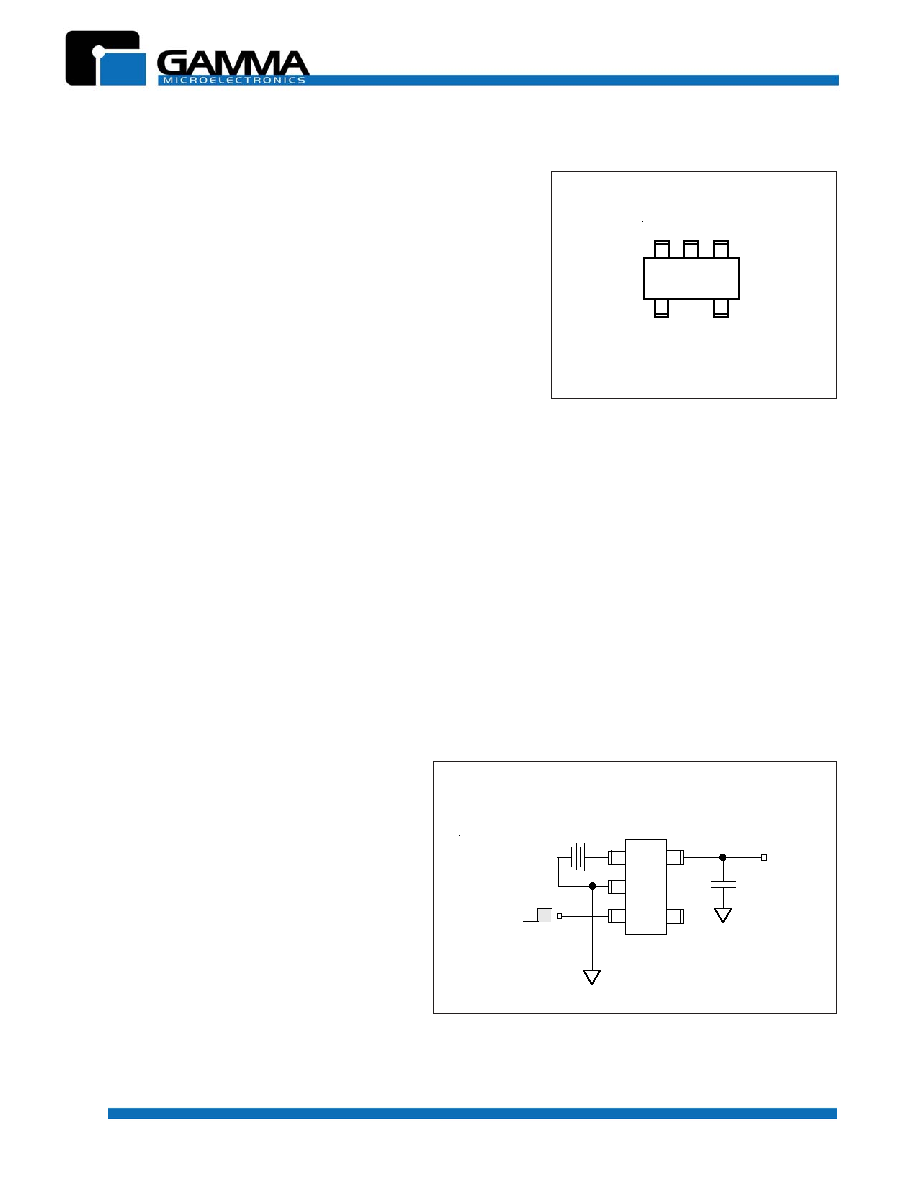
PIN CONFIGURATION
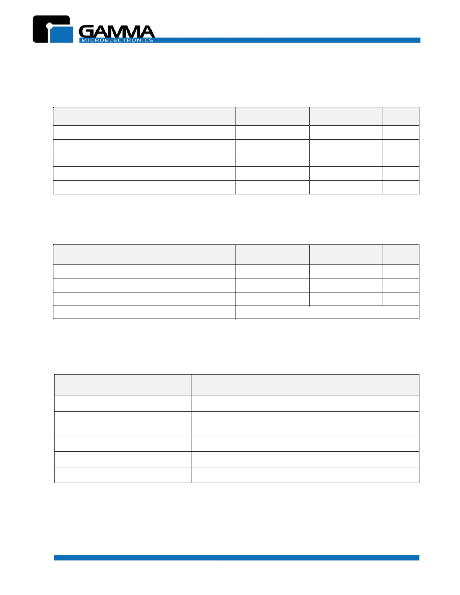
TYPICAL APPLICATION CIRCUIT
Wide Selection of Output Voltages
Guaranteed 80mA Output
Low Quiescent Current
Low Dropout Voltage
Tight Load and Line Regulation
Low Temperature Coefficient
Current and Thermal Limiting
Reversed Input Polarity Protection
Zero OFF-Mode Current
Logic-Controlled Shutdown
SOT-23-5 Package
Applications:
Cellular Phones
Notebook Computers
Palmtops and PDA's
Battery-Powered Equipment
Bar Code Scanners
High-Efficiency Linear Power
Supplies
SMPS Post-Regulator/
DC-to-DC Modules
GND
NC
EN
IN
OUT
SOT-23-5
3
2
1
5
4
The GM6081 is an 80mA linear voltage regulator with very low dropout voltage (from typically 20mV at light
loads to 300mV at 80mA) and very low ground current (225
µ
A at 20mA output). It includes a logic-compatible
enable input and provides better than 3% initial accuracy.
GM6081 is designed for optimal performance with low-value, low-cost ceramic capacitors. In most applications
only 0.47
µ
F of output capacitance is required for stability. The GM6081 is designed specifically for battery-
powered devices. Itcan be controlled by a CMOS or TTL compatible logic signal. When disabled, power
consumption drops practically to zero. If on-off control is not required, the enable pin may be tied to the input
for 3-terminal operation. To further enhance battery life, the ground current of the GM6081 increases only
slightly in dropout.Notable features of the GM6081 include current limiting, overtemperature shutdown, and
protection against reversed battery connection.
The GM6081 is available in 2.8V, 3.0V, 3.3V, 3.6V, 3.8V, 4.0V, 4.5V, 4.75V, and 5.0V fixed voltages. Other
voltages are available by special order.
(Top View)
+
2
1
3
4
5
0.47
µ
F
V
O UT
Enable
Shutdown
SOT-23-5
Revision 1, May 2002 www.gammamicro.com
80mA LOW-DROPOUT LINEAR VOLTAGE REGULATORS
GM6081
PRELIMINARY
2
r
e
t
e
m
a
r
a
P
l
o
b
m
y
S
e
u
l
a
V
t
i
n
U
r
e
w
o
P
n
o
it
a
p
i
s
s
i
D
P
D
d
e
ti
m
il
y
ll
a
n
r
e
t
n
I
W
e
g
a
tl
o
V
y
l
p
p
u
S
t
u
p
n
I
V
N
I
0
2
+
o
t
0
2
-
V
e
g
a
tl
o
V
t
u
p
n
I
e
l
b
a
n
E
V
N
E
0
2
+
o
t
0
2
-
V
)
c
e
s
5
,
g
n
ir
e
d
l
o
S
(
e
r
u
t
a
r
e
p
m
e
T
d
a
e
L
T
D
A
E
L
0
6
2
C
∞
e
g
n
a
R
e
r
u
t
a
r
e
p
m
e
T
e
g
a
r
o
t
S
T
G
T
S
0
5
1
+
o
t
0
6
≠
C
∞
r
e
t
e
m
a
r
a
P
l
o
b
m
y
S
e
u
l
a
V
t
i
n
U
e
g
a
tl
o
V
t
u
p
n
I
V
N
I
6
1
o
t
5
.
2
V
e
g
a
tl
o
V
t
u
p
n
I
e
l
b
a
n
E
V
N
E
V
o
t
0
N
I
V
e
g
n
a
R
e
r
u
t
a
r
e
p
m
e
T
n
o
it
c
n
u
J
T
J
5
2
1
+
o
t
0
4
≠
C
∞
e
c
n
a
t
s
i
s
e
R
l
a
m
r
e
h
T
3
e
t
o
N
PIN FUNCTIONS DESCRIPTION
N
I
P
n
o
i
t
c
n
u
F
n
o
i
t
p
i
r
c
s
e
D
2
D
N
G
d
n
u
o
r
G
3
N
E
h
g
i
h
c
i
g
o
L
.t
u
p
n
i
l
o
r
t
n
o
c
e
l
b
it
a
p
m
o
c
S
O
M
C
/
L
T
T
:
)
t
u
p
n
I
(
e
l
b
a
n
E
.
n
w
o
d
t
u
h
s
=
n
e
p
o
r
o
w
o
l
c
i
g
o
l
;
d
e
l
b
a
n
e
=
1
N
I
t
u
p
n
I
y
l
p
p
u
S
4
C
N
d
e
t
c
e
n
n
o
c
y
ll
a
n
r
e
t
n
i
t
o
n
5
T
U
O
t
u
p
t
u
O
r
o
t
a
l
u
g
e
R
OPERATING RATINGS
ABSOLUTE MAXIMUM
RATINGS
Revision 1, May 2002 www.gammamicro.com
80mA LOW-DROPOUT LINEAR VOLTAGE REGULATORS
GM6081
PRELIMINARY
3
ELECTRICAL CHARACTERISTICS
V
IN
= V
OUT
+ 1V; I
L
= 1mA; C
L
= 0.47
µ
F; V
EN
2.0V; T
J
= 25∞C, bold values indicate ≠40∞C
T
J
+125∞C; unless noted.
r
e
t
e
m
a
r
a
P
l
o
b
m
y
S
s
n
o
i
t
i
d
n
o
C
N
I
M
P
Y
T
X
A
M
t
i
n
U
y
c
a
r
u
c
c
A
e
g
a
tl
o
V
t
u
p
t
u
O
V
O
3
-
4
-
3
4
%
%
t
n
e
i
c
if
f
e
o
C
e
r
u
t
a
r
e
m
e
T
e
g
a
tl
o
V
t
u
p
t
u
O
V
O
/
T
e
t
o
N
4
0
5
0
0
2
m
p
p
C
∞
/
n
o
it
a
l
u
g
e
R
e
n
i
L
V
O
/
V
O
V
N
I
V
=
T
U
O
V
6
1
o
t
V
1
+
8
0
.
0
3
.
0
5
.
0
%
%
n
o
it
a
l
u
g
e
R
d
a
o
L
V
O
/
V
O
I
L
,
A
m
0
8
o
t
A
m
1
.
0
=
e
t
o
N
5
8
0
.
0
3
.
0
5
.
0
%
%
7
e
t
o
N
,
e
g
a
tl
o
V
t
u
o
p
o
r
D
V
N
I
-V
O
I
L
0
0
1
=
µ
A
0
2
V
m
I
L
A
m
0
2
=
0
0
2
0
5
3
V
m
I
L
A
m
0
5
=
0
5
2
V
m
I
L
A
m
0
8
=
0
0
3
0
0
6
V
m
t
n
e
r
r
u
C
t
n
e
c
s
e
i
u
Q
Q
I
V
N
E
)
n
w
o
d
t
u
h
s
(
V
4
.
0
1
0
.
0
0
1
µ
A
8
e
t
o
N
,t
n
e
r
r
u
C
n
i
P
d
n
u
o
r
G
I
D
N
G
I
L
0
0
1
=
µ
V
,
A
N
E
)
e
v
it
c
a
(
V
0
.
2
0
8
1
µ
A
I
L
V
,
A
m
0
2
=
N
E
)
e
v
it
c
a
(
V
0
.
2
5
2
2
0
5
7
µ
A
I
L
V
,
A
m
0
5
=
N
E
)
e
v
it
c
a
(
V
0
.
2
0
5
8
µ
A
I
L
V
,
A
m
0
8
=
N
E
)
e
v
it
c
a
(
V
0
.
2
0
0
8
1
0
0
0
3
µ
A
t
u
o
p
o
r
D
t
a
t
n
e
r
r
u
C
n
i
P
d
n
u
o
r
G
I
O
D
D
N
G
V
N
I
V
=
T
U
O
)l
a
n
i
m
o
n
(
,
V
5
.
0
-
e
t
o
N
7
0
0
2
0
0
3
µ
A
ti
m
i
L
t
n
e
r
r
u
C
I
T
I
M
I
L
V
T
U
O
V
0
=
0
8
1
0
5
2
A
m
n
o
it
a
l
u
g
e
R
l
a
m
r
e
h
T
V
O
/
P
D
e
t
o
N
8
5
0
.
0
W
/
%
t
u
p
n
I
e
l
b
a
n
E
l
e
v
e
L
e
g
a
tl
o
V
t
u
p
n
I
e
l
b
a
n
E
V
L
I
)
F
F
O
(
w
o
L
c
i
g
o
L
6
.
0
V
V
H
I
)
N
O
(
h
g
i
H
c
i
g
o
L
0
.
2
V
t
n
e
r
r
u
C
t
u
p
n
I
e
l
b
a
n
E
V
L
I
V
L
I
6
.
0
V
1
0
.
0
1
µ
A
V
H
I
V
H
I
V
0
.
2
5
1
0
5
µ
A
Note 1. Exceeding the absolute maximum rating may damage the device.
Note 2. The device is not guaranteed to function outside its operating rating.
Note 3: The maximum allowable power dissipation is a function of the maximum junction temperature, T
J(max)
, the junction-to-
ambient thermal resistance,
JA
, and the ambient temperature, T
A
. The maximum allowable power dissipation at any ambient
temperature is calculated using: P
D(max)
= (T
J(max)
≠ T
A
)
˜
JA
. Exceeding the maximum allowable power dissipation will result in
excessive die temperature, and regulator will go into thermal shutdown.
JA
of the SOT-23-5 is 220∞C/W, and 250∞C/W for SOT-143
mounted on a PC (printed circuit) board.
Note 4: Output voltage temperature coefficient is defined as the worst case voltage change divided by the total temperature range.
Note 5: Regulation is measured at constant junction temperature using low duty cycle pulse testing. Parts are tested for load
regulation in the load range from 0.1mA to 150mA. Changes in output voltage due to heating effects are covered by the thermal
regulation specification.
Note 6: Dropout voltage is defined as the input to output differential at which the output voltage drops 2% below its nominal value
measured at 1V differential.
Note 7: Ground PIN current is the regulator quiescent current plus pass transistor base current. The total current drawn from the
supply is the sum ofthe load current plus the ground pin current.
Note 8: Thermal regulation is defined as the change in output voltage at a time "t" after a change in power dissipation is applied,
excluding load or lineregulation effects. Specifications are for an 80mA load pulse at V
IN
= 16V for t = 10ms.
Revision 1, May 2002 www.gammamicro.com
80mA LOW-DROPOUT LINEAR VOLTAGE REGULATORS
GM6081
PRELIMINARY
4
APPLICATIONS INFORMATION
Input Capacitor
Place a 0.1
µ
F capacitor from IN to GND in applications where there is more than 10 inches of wire between
the input and the AC filter capacitor, or where a battery is used as the input.
Output Capacitor
As with any PNP-based regulator, the GM6081 requires an output capacitor to prevent oscillation. However,
the GM6081 is extremely stable, and requires only 0.47
µ
F of output capacitance for stability. You can use the
GM6081 with any type of capacitor, but it works great with cheap, tiny ceramic capacitiors--so, why spend
more? You can increase the output capacitor value without limit to improve transient response.
Caveat: Use a capacitor with a resonant frequency above 500kHz. Ceramic capacitors work great, but some
dielectrics have poor temperature coefficients, which affect the capacitance value over temperature. Tantalum
capacitors are very stable over temperature, but are larger and much more expensive. Aluminum electrolytic
capacitors also work, but they have electrolytes which freeze at ~ ≠30∞C. So, use tantalum or ceramic capacitors
for operation below ≠25∞C.
No-Load Stability
Unlike most regulators, the GM6081 will remain stable and in regulation with no load other than the internal
voltage divider. This makes the GM6081 ideal for CMOS RAM keep-alive applications.
Enable Input
The GM6081 has practically zero off-mode current. When the enable input (EN) is held below 0.6V, the
GM6081 is powered off. Pulling EN high (over 2.0V) turns on the GM6081. When EN is held low, the regulator
typically draws only 15nA of current. While the logic threshold is TTL/CMOS compatible, EN may be pulled as
high as 20V, independent of V
IN
.
1
8
0
6
M
G
E
G
A
K
C
A
P
e
g
a
tl
o
V
t
u
p
t
u
O
5
-
3
2
-
T
O
S
V
8
.
2
V
0
.
3
V
3
.
3
V
6
.
3
V
8
.
3
5
3
2
T
S
8
.
2
-
1
8
0
6
M
G
5
3
2
T
S
0
.
3
-
1
8
0
6
M
G
5
3
2
T
S
3
.
3
-
1
8
0
6
M
G
5
3
2
T
S
6
.
3
-
1
8
0
6
M
G
5
3
2
T
S
8
.
3
-
1
8
0
6
M
G
V
0
.
4
V
5
.
4
V
5
7
.
4
V
0
.
5
J
D
A
5
3
2
T
S
0
.
4
-
1
8
0
6
M
G
5
3
2
T
S
5
.
4
-
1
8
0
6
M
G
5
3
2
T
S
5
7
.
4
-
1
8
0
6
M
G
5
3
2
T
S
0
.
5
-
1
8
0
6
M
G
-
ORDERING INFORMATION
Revision 1, May 2002 www.gammamicro.com
80mA LOW-DROPOUT LINEAR VOLTAGE REGULATORS
GM6081
PRELIMINARY
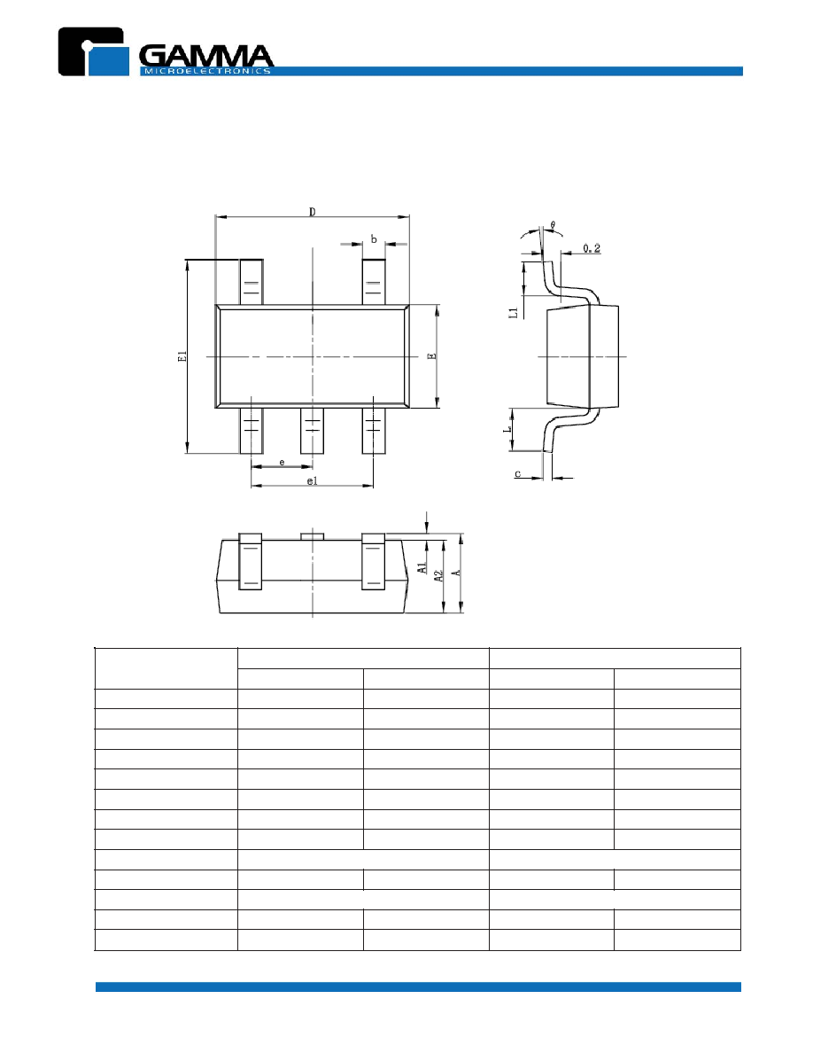
5
SOT-23-5 PACKAGE OUTLINE DIMENSIONS
L
O
B
M
Y
S
s
r
e
t
e
m
il
li
M
n
I
s
n
o
i
s
n
e
m
i
D
s
e
h
c
n
I
n
I
s
n
o
i
s
n
e
m
i
D
N
I
M
X
A
M
N
I
M
X
A
M
A
0
5
0
.
1
0
5
2
.
1
1
4
0
.
0
9
4
0
.
0
1
A
0
0
0
.
0
0
0
1
.
0
0
0
0
.
0
4
0
0
.
0
2
A
0
5
0
.
1
0
5
1
.
1
1
4
0
.
0
5
4
0
.
0
b
0
0
3
.
0
0
0
4
.
0
2
1
0
.
0
6
1
0
.
0
c
0
0
1
.
0
0
0
2
.
0
4
0
0
.
0
8
0
0
.
0
D
0
2
8
.
2
0
2
0
.
3
1
1
1
.
0
9
1
1
.
0
E
0
0
5
.
1
0
0
7
.
1
9
5
0
.
0
7
6
0
.
0
1
E
0
5
6
.
2
0
5
9
.
2
4
0
1
.
0
6
1
1
.
0
e
P
Y
T
0
5
9
.
0
P
Y
T
7
3
0
.
0
1
e
0
0
8
.
1
0
0
0
.
2
1
7
0
.
0
9
7
0
.
0
L
F
E
R
0
0
7
.
0
F
E
R
8
2
0
.
0
1
L
0
0
3
.
0
0
0
6
.
0
2
1
0
.
0
4
2
0
.
0
∞
0
∞
8
∞
0
∞
8