GM6150
ULTRA-LOW DROPOUT CMOS VOLTAGE REGULATORS
Revision 1, May 2002 www.gammamicro.com
PRELIMINARY
Maximum output current 150mA (V
OUT
= 3.0V)
Output voltage 1.8V to 6.0V in 0.1V increments
Output voltage
±
2%
CMOS Low power consumption
Input stability typ. 0.2%/V
Ultra-low dropout voltage (typ. 0.20V at 80mA, 0.38V at 160mA)
Stand-by current 0.1
µ
A (V
OUT
= 3.0V)
SOT-25 (150mW) and SOT-89 (500mW) packages
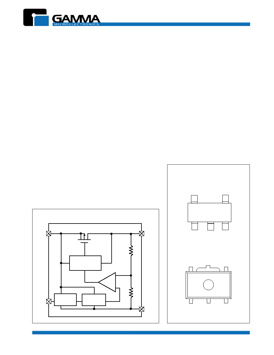
The GM6150's combine high accuracy with very low power consumption, providing high output current even when
the application requires very low dropout voltage. The Chip Enable (CE) input allows the output to be turned off to
prolong battery life. The GM6150's include a precision voltage reference, error correction circuitry, and a current-
limited output driver. Fast transient response to load variations provides excellent stability under dynamic load
conditions. The CE function in the GM6150's is positive logic; also available are the GM6152's with negative logic.
The GM6150 is available in fixed output voltages from 1.8V to 6.0V in 0.1V increments, and in SOT-25 (150mW)
and SOT-89 (500mW) packages.
SOT-25 (TOP VIEW)
PIN CONFIGURATIONS
PDA's
Cameras and camcorders
VCR's
Battery Powered Equipment
Voltage Supply for Cellular Phones
Applications:
BLOCK DIAGRAM
1
V
IN
V
OUT
V
SS
+
-
Current
Limit
Voltage
Reference
SOT-89-5 (TOP VIEW)
V
SS
V
OUT
V
IN
1
3
2
1
2
3
V
SS
V
OUT
V
IN
5
4
CE
(NC)
(NC)
CE
Output
Current
CE
5
4
GM6150
ULTRA-LOW DROPOUT CMOS VOLTAGE REGULATORS
Revision 1, May 2002 www.gammamicro.com
PRELIMINARY
2
R
E
B
M
U
N
N
I
P
E
M
A
N
N
I
P
N
O
I
T
C
N
U
F
5
2
-
T
O
S
5
-
9
8
-
T
O
S
1
4
V
S
S
d
n
u
o
r
G
2
2
V
N
I
t
u
p
n
i
e
g
a
tl
o
v
y
l
p
p
u
S
3
3
E
C
e
l
b
a
n
E
p
i
h
C
4
1
)
C
N
(
n
o
it
c
e
n
n
o
c
o
N
5
5
V
T
U
O
t
u
p
t
u
o
e
g
a
tl
o
v
d
e
t
a
l
u
g
e
R
PIN ASIGNMENTS
R
E
T
E
M
A
R
A
P
L
O
B
M
Y
S
S
G
N
I
T
A
R
S
T
I
N
U
e
g
a
tl
o
V
t
u
p
n
I
V
N
I
2
1
V
e
g
a
tl
o
V
t
u
p
t
u
O
V
T
U
O
V
S
S
V
~
3
.
0
≠
N
I
3
.
0
+
V
e
g
a
tl
o
V
t
u
p
n
I
E
C
V
E
C
V
S
S
V
~
3
.
0
≠
N
I
3
.
0
+
V
t
n
e
r
r
u
C
t
u
p
t
u
O
I
T
U
O
0
0
5
A
m
s
u
o
n
it
n
o
C
n
o
it
a
p
i
s
s
i
D
r
e
w
o
P
l
a
t
o
T
5
2
-
T
O
S
P
d
0
5
1
W
m
5
-
9
8
-
T
O
S
0
0
5
e
r
u
t
a
r
e
p
m
e
T
t
n
e
i
b
m
A
g
n
it
a
r
e
p
O
T
r
p
o
5
8
+
~
0
4
≠
C
∞
e
r
u
t
a
r
e
p
m
e
T
e
g
a
r
o
t
S
T
g
t
s
5
2
1
+
~
0
4
≠
C
∞
ABSOLUTE MAXIMUM RATINGS
T
A
=25
∞
C
ORDERING INFORMATION
0
5
1
6
M
G
E
G
A
K
C
A
P
e
g
a
tl
o
V
t
u
p
t
u
O
V
5
.
2
V
0
.
3
V
3
.
3
*
r
e
h
t
O
5
2
-
T
O
S
5
2
T
S
5
.
2
-
0
5
1
6
M
G
5
2
T
S
0
.
3
-
0
5
1
6
M
G
5
2
T
S
3
.
3
-
0
5
1
6
M
G
5
2
T
S
x
.
x
-
0
5
1
6
M
G
5
-
9
8
-
T
O
S
5
-
9
8
T
S
5
.
2
-
0
5
1
6
M
G
5
-
9
8
T
S
0
.
3
-
0
5
1
6
M
G
5
-
9
8
T
S
3
.
3
-
0
5
1
6
M
G
5
-
9
8
T
S
x
.
x
-
0
5
1
6
M
G
* x.x Denotes output voltages from 1.8V to 6.0V in 0.1V increments.
GM6150
ULTRA-LOW DROPOUT CMOS VOLTAGE REGULATORS
Revision 1, May 2002 www.gammamicro.com
PRELIMINARY
3
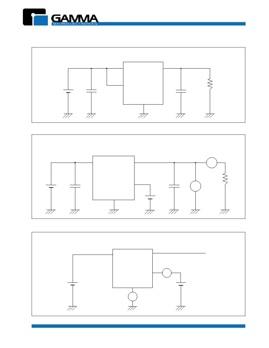
STANDARD CIRCUIT
V
IN
V
OUT
V
SS
V
IN
C
IN
C
L
R
L
4.7
µ
F
(Tantalum)
1
µ
F
(Tantalum)
CE
Typical Application Circuit 1
V
IN
4.7
µ
F
(Tantalum)
10
µ
F
(Tantalum)
V
A
V
IN
V
OUT
V
SS
CE
V
CE
Typical Application Circuit 2
V
IN
Open
V
IN
V
OUT
V
SS
A
CE
A
V
CE
GM6150
ULTRA-LOW DROPOUT CMOS VOLTAGE REGULATORS
Revision 1, May 2002 www.gammamicro.com
PRELIMINARY
4
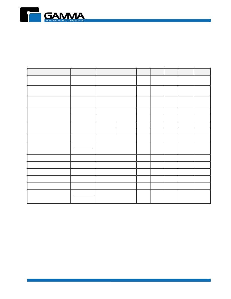
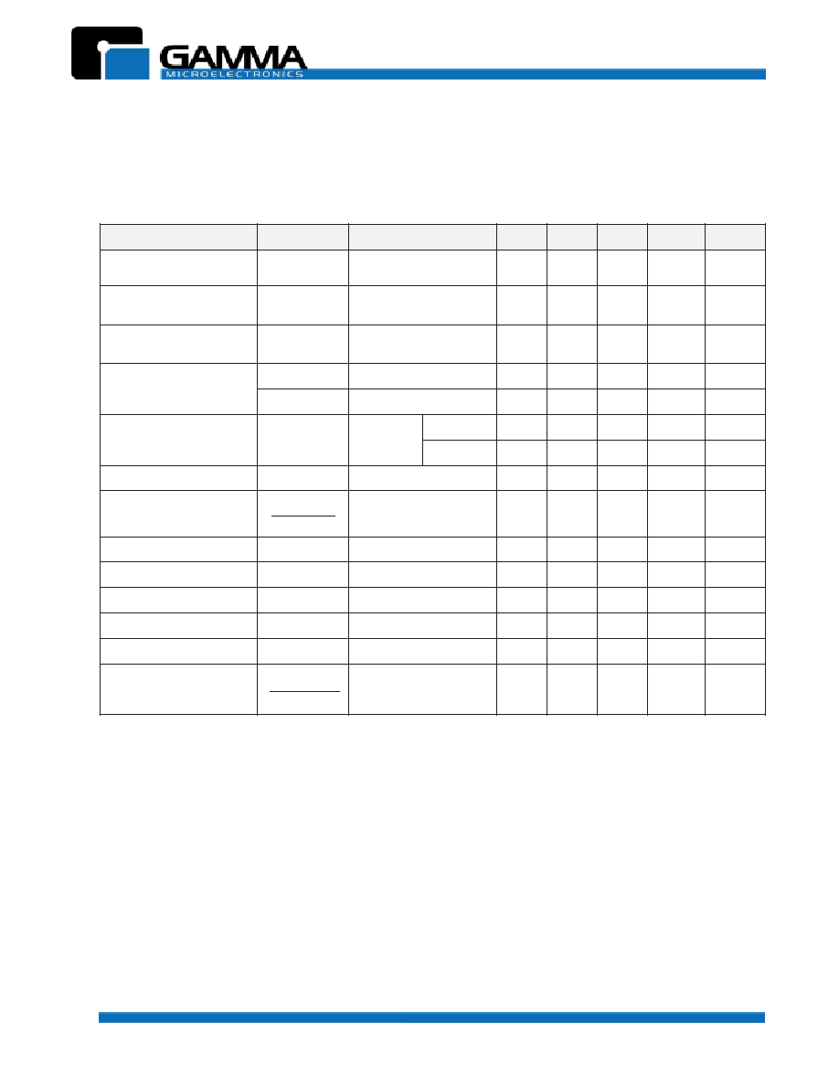
ELECTRICAL CHARACTERISTICS
(T
A
= 25∫ C unless otherwise noted)
GM6150 - 3.0 (V
OUT
(T)=3.0V) - Note 1
R
E
T
E
M
A
R
A
P
L
O
B
M
Y
S
S
N
O
I
T
I
D
N
O
C
N
I
M
P
Y
T
X
A
M
S
T
I
N
U
T
I
U
C
R
I
C
e
g
a
tl
o
V
t
u
p
t
u
O
V
T
U
O
)
E
(
)
2
e
t
o
n
(
I
T
U
O
,
A
m
0
4
=
V
N
I
V
0
.
4
=
0
4
9
.
2
0
0
0
.
3
0
6
0
.
3
V
1
t
n
e
r
r
u
C
t
u
p
t
u
O
m
u
m
i
x
a
M
I
T
U
O
x
a
m
V
N
I
V
0
.
4
=
V
T
U
O
)
E
(
$
V
7
.
2
0
5
1
A
m
1
y
ti
li
b
a
t
S
d
a
o
L
™
™
™
™
™
V
T
U
O
V
N
I
V
0
.
4
=
A
m
1
#
I
T
U
O
#
A
m
0
8
5
4
0
9
V
m
1
t
u
p
u
O
-
t
u
p
n
I
l
a
it
n
e
r
e
ff
i
D
e
g
a
tl
o
V
1
fi
d
V
I
T
U
O
A
m
0
8
=
0
0
2
5
9
3
V
m
1
2
fi
d
V
I
T
U
O
A
m
0
6
1
=
0
8
3
0
7
7
V
m
1
1
t
n
e
r
r
u
C
y
l
p
p
u
S
I
S
S
1
V
N
I
V
=
E
C
V
0
.
4
=
1
1
9
1
:
A
2
3
2
1
3
:
A
2
2
t
n
e
r
r
u
C
y
l
p
p
u
S
I
S
S
2
V
N
I
V
,
V
0
.
4
=
E
C
V
=
S
S
1
.
0
:
A
2
y
ti
li
b
a
t
S
t
u
p
n
I
™
™
™
™
™
V
T
U
O
™
™
™
™
™
V
N
I
C
C
C
C
C
™
™
™
™
™
V
T
U
O
I
T
U
O
A
m
0
4
=
V
0
.
4
#
V
N
I
#
V
0
.
0
1
2
.
0
3
.
0
V
/
%
1
e
g
a
tl
o
V
t
u
p
n
I
V
N
I
0
.
0
1
V
--
"
h
g
i
H
"
e
g
a
tl
o
V
t
u
p
n
I
E
C
V
H
E
C
5
.
1
V
1
"
w
o
L
"
e
g
a
tl
o
V
t
u
p
n
I
E
C
V
L
E
C
5
2
.
0
V
1
"
h
g
i
H
"
t
n
e
r
r
u
C
t
u
p
n
I
E
C
I
H
E
C
V
E
C
V
=
N
I
0
.
5
:
A
2
"
w
o
L
"
t
n
e
r
r
u
C
t
u
p
n
I
E
C
I
L
E
C
V
E
C
V
=
N
I
2
.
0
-
5
0
.
0
-
0
:
A
2
e
g
a
tl
o
V
t
u
p
t
u
O
s
c
it
s
ir
e
t
c
a
r
a
h
C
e
r
u
t
a
r
e
p
m
e
T
™
™
™
™
™
V
T
U
O
™
™
™
™
™
T
R
P
O
C
C
C
C
C
™
™
™
™
™
V
T
U
O
I
T
U
O
A
m
0
4
=
C
∫
0
3
-
#
T
R
P
O
#
C
∫
5
8
K 0
0
1
C
∫
/
m
p
p
1
1. V
OUT
(T)=Specified Output Voltage
2. V
OUT
(E)=Effective Output Voltage (the output voltage when "V
OUT
(T) + 1.0V" is provided at the V
IN
pin while maintaining a certain I
OUT
value)
3. Vdif= {V
IN
1 (Note5)-V
OUT
1(Note4) }
4.
V
OUT
1= A voltage equal to 98% of the Output Voltage whenever an amply stabilised I
OUT
{V
OUT
(T)+1.0V} is input.
5. V
IN
1= The input voltage at the time 98% of V
OUT
(E) is output (input voltage has been gradually reduced).
6. High speed is Semi-custom.
Note:
(Note6)
Standard
High Speed
Other Output Voltages from 1.8V to 6.0V are available in 0.1V increments.
GM6150
ULTRA-LOW DROPOUT CMOS VOLTAGE REGULATORS
Revision 1, May 2002 www.gammamicro.com
PRELIMINARY
5
GM6150 - 5.0 (V
OUT
(T)=5.0V) - Note 1
R
E
T
E
M
A
R
A
P
L
O
B
M
Y
S
S
N
O
I
T
I
D
N
O
C
N
I
M
P
Y
T
X
A
M
S
T
I
N
U
T
I
U
C
R
I
C
e
g
a
tl
o
V
t
u
p
t
u
O
V
T
U
O
)
E
(
)
2
e
t
o
n
(
I
T
U
O
,
A
m
0
4
=
V
N
I
V
0
.
6
=
0
0
9
.
4
0
0
0
.
5
0
0
1
.
5
V
1
t
n
e
r
r
u
C
t
u
p
t
u
O
m
u
m
i
x
a
M
I
T
U
O
x
a
m
V
N
I
V
0
.
6
=
V
T
U
O
)
E
(
$
V
5
.
4
0
8
1
A
m
1
y
ti
li
b
a
t
S
d
a
o
L
™
™
™
™
™
V
T
U
O
V
N
I
V
0
.
6
=
A
m
1
#
I
T
U
O
#
A
m
0
0
1
0
4
0
8
V
m
1
t
u
p
u
O
-
t
u
p
n
I
l
a
it
n
e
r
e
ff
i
D
e
g
a
tl
o
V
1
fi
d
V
I
T
U
O
A
m
0
0
1
=
5
6
1
0
3
3
V
m
1
2
fi
d
V
I
T
U
O
A
m
0
0
2
=
0
3
3
0
6
6
V
m
1
1
t
n
e
r
r
u
C
y
l
p
p
u
S
I
S
S
1
V
N
I
V
=
E
C
V
0
.
6
=
3
1
1
2
:
A
2
7
2
5
3
:
A
2
2
t
n
e
r
r
u
C
y
l
p
p
u
S
I
S
S
2
V
N
I
V
,
V
0
.
6
=
E
C
V
=
S
S
1
.
0
:
A
2
y
ti
li
b
a
t
S
t
u
p
n
I
™
™
™
™
™
V
T
U
O
™
™
™
™
™
V
N
I
C
C
C
C
C
™
™
™
™
™
V
T
U
O
I
T
U
O
A
m
0
4
=
V
0
.
6
#
V
N
I
#
V
0
.
0
1
2
.
0
3
.
0
V
/
%
1
e
g
a
tl
o
V
t
u
p
n
I
V
N
I
0
.
0
1
V
--
"
h
g
i
H
"
e
g
a
tl
o
V
t
u
p
n
I
E
C
V
H
E
C
5
.
1
V
1
"
w
o
L
"
e
g
a
tl
o
V
t
u
p
n
I
E
C
V
L
E
C
5
2
.
0
V
1
"
h
g
i
H
"
t
n
e
r
r
u
C
t
u
p
n
I
E
C
I
H
E
C
V
E
C
V
=
N
I
0
.
5
:
A
2
"
w
o
L
"
t
n
e
r
r
u
C
t
u
p
n
I
E
C
I
L
E
C
V
E
C
V
=
N
I
2
.
0
-
5
0
.
0
-
0
:
A
2
e
g
a
tl
o
V
t
u
p
t
u
O
s
c
it
s
ir
e
t
c
a
r
a
h
C
e
r
u
t
a
r
e
p
m
e
T
™
™
™
™
™
V
T
U
O
™
™
™
™
™
T
R
P
O
C
C
C
C
C
™
™
™
™
™
V
T
U
O
I
T
U
O
A
m
0
4
=
C
∫
0
3
-
#
T
R
P
O
#
C
∫
5
8
K 0
0
1
C
∫
/
m
p
p
1
1. V
OUT
(T)=Specified Output Voltage
2. V
OUT
(E)=Effective Output Voltage (the output voltage when "V
OUT
(T) + 1.0V" is provided at the V
IN
pin while maintaining a certain I
OUT
value)
3. Vdif= {V
IN
1 (Note5)-V
OUT
1(Note4) }
4.
V
OUT
1= A voltage equal to 98% of the Output Voltage whenever an amply stabilised I
OUT
{V
OUT
(T)+1.0V} is input.
5. V
IN
1= The input voltage at the time 98% of V
OUT
(E) is output (input voltage has been gradually reduced).
6. High speed is Semi-custom.
Note:
(Note6)
Standard
High Speed
ELECTRICAL CHARACTERISTICS
(T
A
= 25∫ C unless otherwise noted)
Other Output Voltages from 1.8V to 6.0V are available in 0.1V increments.