GM6155
150mA LOW-NOISE LDO REGULATOR
Revision 1, November 2002 1 www.gammamicro.com
PRELIMINARY
The GM6155 is an efficient linear voltage regulator with ultralow-noise output, very low dropout voltage (typically
17mV at light loads and 100mV at 50mA), and very low ground current (600
µ
A at 100mA output). The GM6155
provides better than 1% initial accuracy.
Designed especially for hand-held, battery-powered devices, the GM6155 includes a CMOS or TTL compatible
enable/shutdown control input. When shutdown, power consumption drops nearly to zero. Regulator ground
current increases only slightly in dropout, further prolonging battery life. Key GM6155 features include a reference
bypass pin to improve its already excellent low-noise performance, reversed-battery protection, current limiting,
and overtemperature shutdown.
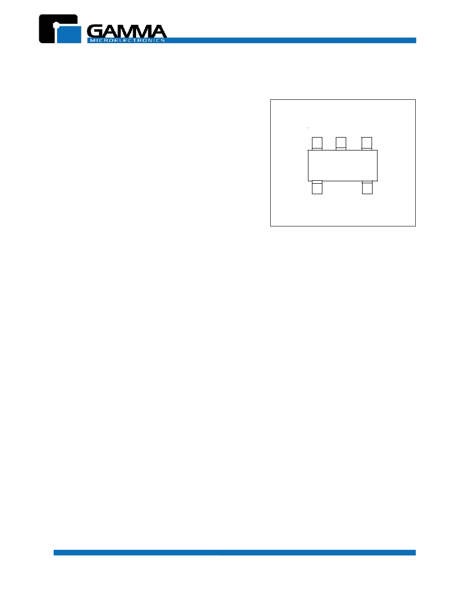
The GM6155-3.3 is available in SOT-23-5 package.
Very low noise output
Extremely accurate output voltage
Guaranteed 150mA output
Low quiescent current
Low dropout voltage
Extremely tight load and line regulation
Very low temperature coefficient
Current and thermal limiting
Reverse-battery protection
"Zero" off-mode current
Logic-controlled electronic enable
Cellular telephones
Laptop, notebook, and palmtop computers
Battery-powered equipment
PCMCIA V
CC
and V
PP
regulation/switching
Consumer/personal electronics
SMPS post-regulator/dc-to-dc modules
High-efficiency linear power supplies
Applications:
3
2
1
4
5
GM6155-3.3
IN
GND
EN
BYP
OUT
SOT-23-5 (TOP VIEW)
PIN CONFIGURATION
GM6155
150mA LOW-NOISE LDO REGULATOR
Revision 1, November 2002 2 www.gammamicro.com
PRELIMINARY
N
I
P
R
E
B
M
U
N
E
M
A
N
N
I
P
N
O
I
T
C
N
U
F
1
N
I
t
u
p
n
I
y
l
p
p
u
S
2
D
N
G
d
n
u
o
r
G
3
N
E
,
e
l
b
a
n
e
=
h
g
i
h
c
i
g
o
L
.t
u
p
n
i
e
l
b
it
a
p
m
o
c
S
O
M
C
:
)
t
u
p
n
I
(
n
w
o
d
t
u
h
S
/
e
l
b
a
n
E
.
n
w
o
d
t
u
h
s
=
n
e
p
o
r
o
w
o
l
c
i
g
o
l
4
P
Y
B
e
c
u
d
e
r
o
t
D
N
G
o
t
r
o
ti
c
a
p
a
c
F
p
0
7
4
l
a
n
r
e
t
x
e
t
c
e
n
n
o
C
:
s
s
a
p
y
B
e
c
n
e
r
e
f
e
R
.
n
e
p
o
tf
e
l
e
b
y
a
M
.
e
s
i
o
n
t
u
p
t
u
o
5
T
U
O
t
u
p
t
u
O
r
o
t
a
l
u
g
e
R
PIN ASIGNMENTS
R
E
T
E
M
A
R
A
P
L
O
B
M
Y
S
S
G
N
I
T
A
R
S
T
I
N
U
e
g
a
tl
o
V
t
u
p
n
I
y
l
p
p
u
S
V
N
I
0
2
+
~
0
2
≠
V
e
g
a
tl
o
V
t
u
p
n
I
e
l
b
a
n
E
V
N
E
0
2
+
~
0
2
≠
V
)
3
e
t
o
N
(
n
o
it
a
p
i
s
s
i
D
r
e
w
o
P
P
D
d
e
ti
m
i
L
y
ll
a
n
r
e
t
n
I
W
e
r
u
t
a
r
e
p
m
e
T
n
o
it
c
n
u
J
T
J
5
2
1
+
~
0
4
≠
C
∞
)
s
d
n
o
c
e
s
5
,
g
n
ir
e
d
l
o
s
(
e
r
u
t
a
r
e
p
m
e
T
d
a
e
L
T
D
A
E
L
0
6
2
C
∞
e
r
u
t
a
r
e
p
m
e
T
e
g
a
r
o
t
S
T
S
0
5
1
+
~
5
6
≠
C
∞
ABSOLUTE MAXIMUM RATINGS (Note 1)
R
E
T
E
M
A
R
A
P
L
O
B
M
Y
S
S
G
N
I
T
A
R
S
T
I
N
U
e
g
a
tl
o
V
t
u
p
n
I
y
l
p
p
u
S
V
N
I
0
2
+
~
0
2
≠
V
e
g
a
tl
o
V
t
u
p
n
I
e
l
b
a
n
E
V
N
E
0
2
+
~
0
2
≠
V
e
r
u
t
a
r
e
p
m
e
T
n
o
it
c
n
u
J
T
J
5
2
1
+
~
0
4
≠
C
∞
e
c
n
a
t
s
i
s
e
R
l
a
m
r
e
h
T
A
J
)
3
e
t
o
N
(
W
/
C
∞
OPERATING RATINGS (Note 2)
GM6155
150mA LOW-NOISE LDO REGULATOR
Revision 1, November 2002 3 www.gammamicro.com
PRELIMINARY
R
E
T
E
M
A
R
A
P
L
O
B
M
Y
S
S
N
O
I
T
I
D
N
O
C
T
S
E
T
N
I
M
P
Y
T
X
A
M
T
I
N
U
y
c
a
r
u
c
c
A
e
g
a
tl
o
V
t
u
p
t
u
O
V
O
V
d
e
if
i
c
e
p
s
m
o
r
f
n
o
it
a
ir
a
V
T
U
O
1
-
2
-
1
2
%
e
r
u
t
a
r
e
p
m
e
T
e
g
a
tl
o
V
t
u
p
t
u
O
t
n
e
i
c
if
f
o
C
V
O
/
T
)
4
e
t
o
N
(
0
0
1
C
∞
/
m
p
p
n
o
it
a
l
u
g
e
R
e
n
i
L
V
O
/
V
O
V
I
N
V
=
T
U
O
V
6
1
o
t
V
1
+
0
1
0
2
V
m
n
o
it
a
l
u
g
e
R
d
a
o
L
V
O
/
V
O
I
L
)
5
e
t
o
N
(
,
A
m
0
5
1
o
t
A
m
1
.
0
=
0
3
0
9
V
m
)
6
e
t
o
N
(
e
g
a
tl
o
V
t
u
o
p
o
r
D
V
N
I
V
-
O
I
L
A
m
0
5
=
0
0
1
0
0
2
V
m
t
n
e
r
r
u
C
t
n
e
c
s
e
i
u
Q
I
D
N
G
V
N
E
)
n
w
o
d
t
u
h
s
(
V
4
.
0
V
N
E
)
n
w
o
d
t
u
h
s
(
V
8
1
.
0
1
0
.
0
1
5
µ
A
)
7
e
t
o
N
(
t
n
e
r
r
u
C
n
i
P
d
n
u
o
r
G
I
D
N
G
V
N
E
I
,
V
0
.
2
L
A
m
1
.
0
=
I
L
A
m
0
5
=
I
L
A
m
0
0
1
=
I
L
A
m
0
5
1
=
0
8
0
5
3
0
0
6
0
0
3
1
5
2
1
0
5
1
0
0
6
0
0
8
0
0
0
1
0
0
5
1
0
0
9
1
0
0
5
2
µ
A
n
o
it
c
e
j
e
R
e
l
p
p
i
R
R
R
S
P
I
,
z
H
0
0
1
=
f
L
A
m
1
.
0
=
5
7
B
d
ti
m
i
L
t
n
e
r
r
u
C
I
T
I
M
I
L
V
T
U
O
V
0
=
0
2
3
0
0
5
A
m
n
o
it
a
l
u
g
e
R
l
a
m
r
e
h
T
V
O
/
P
D
)
8
e
t
o
N
(
5
0
.
0
W
/
%
e
s
i
o
N
t
u
p
t
u
O
e
O
N
I
L
C
,
A
m
0
5
=
L
2
.
2
=
µ
,
F
D
N
G
o
t
P
Y
B
m
o
r
f
F
p
0
7
4
0
6
2
V
n
z
H
t
u
p
n
I
E
L
B
A
N
E
w
o
L
-
c
i
g
o
L
t
u
p
n
I
e
l
b
a
n
E
e
g
a
tl
o
V
V
L
I
n
w
o
d
t
u
h
s
r
o
t
a
l
u
g
e
r
4
.
0
8
1
.
0
V
h
g
i
H
-
c
i
g
o
L
t
u
p
n
I
e
l
b
a
n
E
e
g
a
tl
o
V
V
H
I
d
e
l
b
a
n
e
r
o
t
a
l
u
g
e
r
0
.
2
V
t
n
e
r
r
u
C
t
u
p
n
I
e
l
b
a
n
E
I
L
I
V
L
I
V
4
.
0
V
L
I
V
8
1
.
0
1
0
.
0
1
-
2
-
µ
A
I
H
I
V
H
I
V
0
.
2
2
5
0
2
5
2
ELECTRICAL CHARACTERISTICS
(V
IN
= V
OUT
+ 1V; I
L
= 100
µ
A; C
L
= 1.0
µ
F; V
EN
2.0V;
T
J
= 25∞C, bold values indicate ≠40∞C
T
J
+125∞C; unless otherwise noted)
Note 1. Exceeding the absolute maximum rating may damage the device.
Note 2. The device is not guaranteed to function outside its operating rating.
Note 3: The maximum allowable power dissipation at any T
A
(ambient temperature) is P
D
(max) = (T
J
(max) ≠ T
A
)
JA
. Exceeding the
maximum allowable power dissipation will result in excessive die temperature, and the regulator will go into thermal shutdown.
Note 4: Output voltage temperature coefficient is defined as the worst case voltage change divided by the total temperature range.
Note 5: Regulation is measured at constant junction temperature using low duty cycle pulse testing. Parts are tested for load
regulation in the load range from 0.1mA to 150mA. Changes in output voltage due to heating effects are covered by the thermal
regulation specification.
Note 6: Dropout Voltage is defined as the input to output differential at which the output voltage drops 2% below its nominal value
measured at 1V differential.
Note 7: Ground pin current is the regulator quiescent current plus pass transistor base current. The total current drawn from the
supply is the sum of the load current plus the ground pin current.
Note 8: Thermal regulation is defined as the change in output voltage at a time "t" after a change in power dissipation is applied,
excluding load or line regulation effects. Specifications are for a 150mA load pulse at VIN = 16V for t = 10ms.

GM6155
150mA LOW-NOISE LDO REGULATOR
Revision 1, November 2002 4 www.gammamicro.com
PRELIMINARY
TYPICAL APPLICATION CIRCUIT
2
1
3
4
5
V
O UT
Enable
Shutdown
GM6155-3.3ST5
V
IN
C
BYP
C
OUT
=2.2
µ
F
(tantalum)
EN
EN (pin 3) may be connected
directly to IN (pin 1).
L
ow-Noise Operation:
C
BYP
= 470pF, C
OUT
2.2µF
Basic Operation:
C
BYP
= not used, C
OUT
1µF
GM6155
150mA LOW-NOISE LDO REGULATOR
Revision 1, November 2002 5 www.gammamicro.com
PRELIMINARY
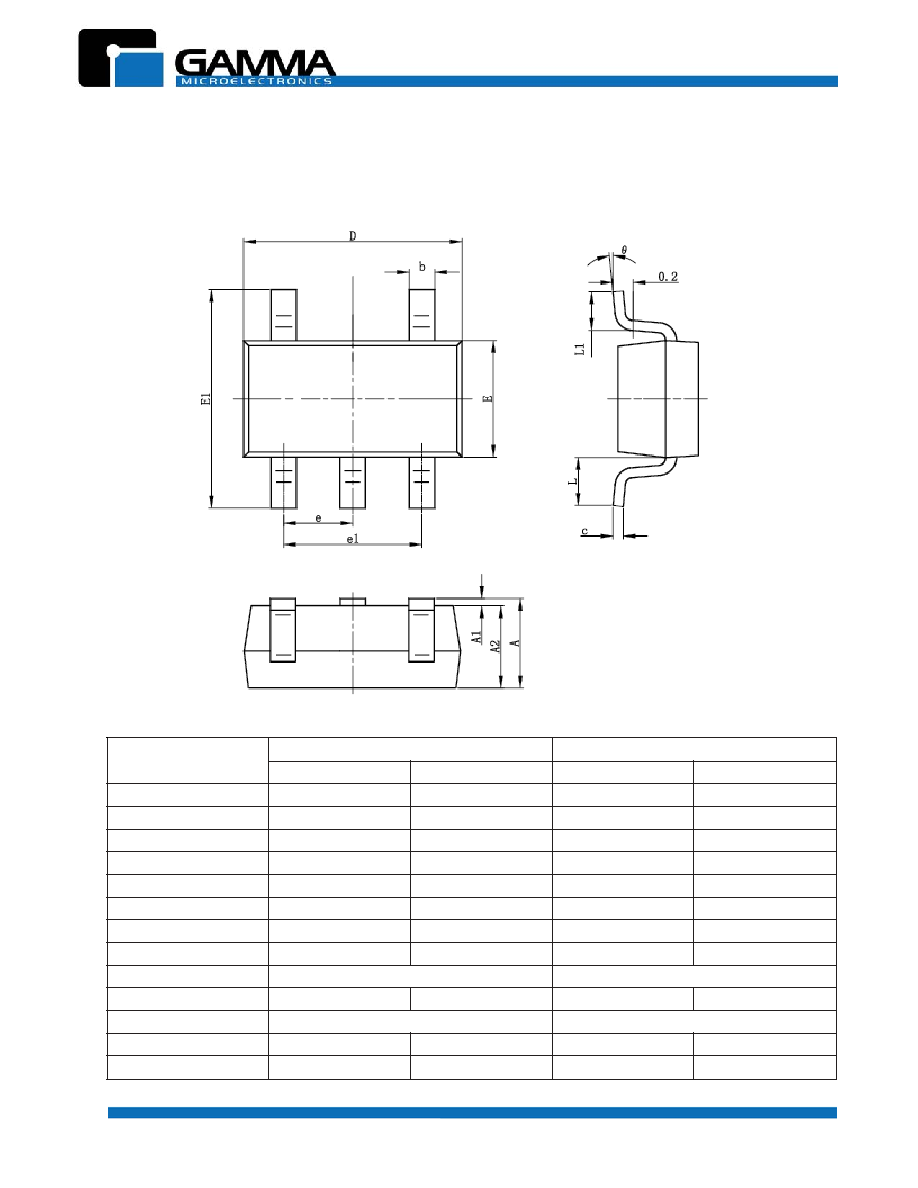
SOT-23-5 PACKAGE OUTLINE DIMENSIONS
L
O
B
M
Y
S
s
r
e
t
e
m
il
li
M
n
I
s
n
o
i
s
n
e
m
i
D
s
e
h
c
n
I
n
I
s
n
o
i
s
n
e
m
i
D
N
I
M
X
A
M
N
I
M
X
A
M
A
0
5
0
.
1
0
5
2
.
1
1
4
0
.
0
9
4
0
.
0
1
A
0
0
0
.
0
0
0
1
.
0
0
0
0
.
0
4
0
0
.
0
2
A
0
5
0
.
1
0
5
1
.
1
1
4
0
.
0
5
4
0
.
0
b
0
0
3
.
0
0
0
4
.
0
2
1
0
.
0
6
1
0
.
0
c
0
0
1
.
0
0
0
2
.
0
4
0
0
.
0
8
0
0
.
0
D
0
2
8
.
2
0
2
0
.
3
1
1
1
.
0
9
1
1
.
0
E
0
0
5
.
1
0
0
7
.
1
9
5
0
.
0
7
6
0
.
0
1
E
0
5
6
.
2
0
5
9
.
2
4
0
1
.
0
6
1
1
.
0
e
P
Y
T
0
5
9
.
0
P
Y
T
7
3
0
.
0
1
e
0
0
8
.
1
0
0
0
.
2
1
7
0
.
0
9
7
0
.
0
L
F
E
R
0
0
7
.
0
F
E
R
8
2
0
.
0
1
L
0
0
3
.
0
0
0
6
.
0
2
1
0
.
0
4
2
0
.
0
∞
0
∞
8
∞
0
∞
8