Revision 2, February 2003 1 www.gammamicro.com
3.0A PRECISION LINEAR REGULATORS
GM6603
PRELIMINARY
Adjustable or Fixed Output
Output Current of 3.0A
Dropout Voltage (typical) 1.2V @ 3.0A
Typical Line Regulation 0.015%
Typical Load Regulation 0.05%
Fast Transient Response
Current Limit Protection
Thermal Shutdown Protection
The GM6603 series of positive adjustable and fixed
regulators are designed to provide 3.0A output with low
dropout voltage performance.
On-chip trimming adjusts the reference voltage to 2.0%.
Put them to work in post regulators or microprocessor
power supplies where low voltage operation and fast
transient response are required.
Device includes over-current protection and thermal
shutdown protection as well.
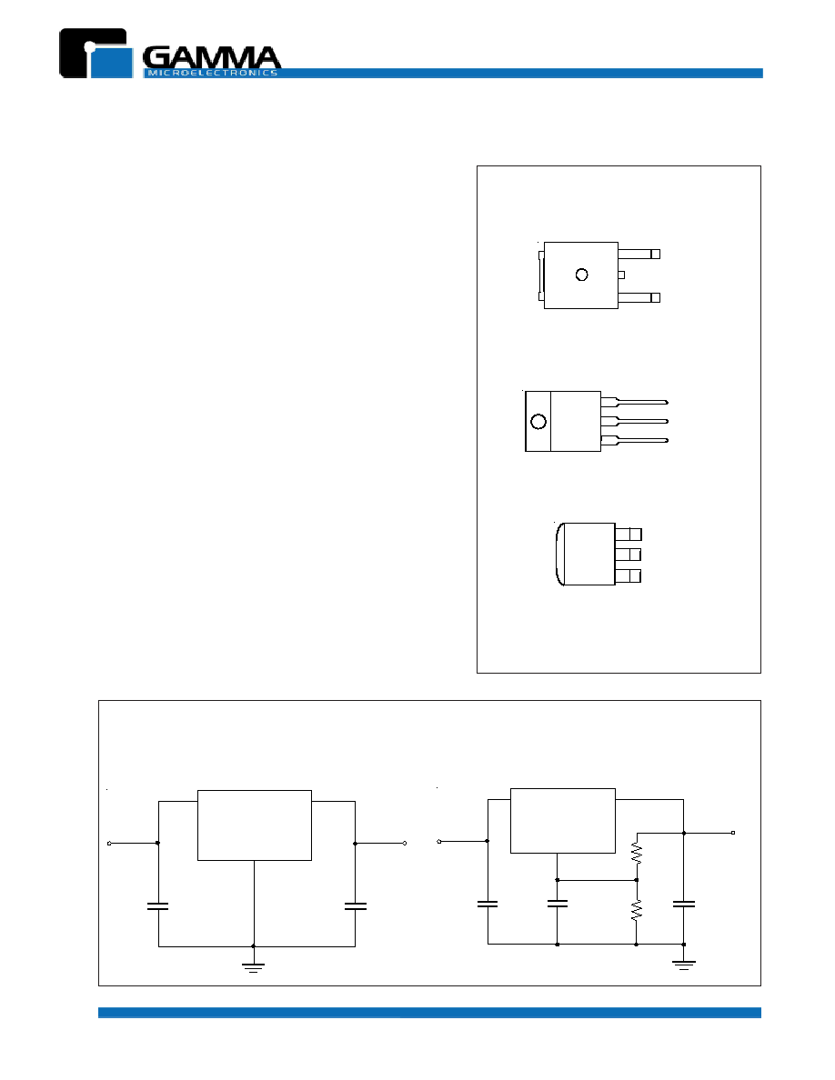
Pin-to-pin compatible with the LT1085 family of
regulators, the GM6603's are available in TO-252,
TO-220 and surface-mount TO263 packages.
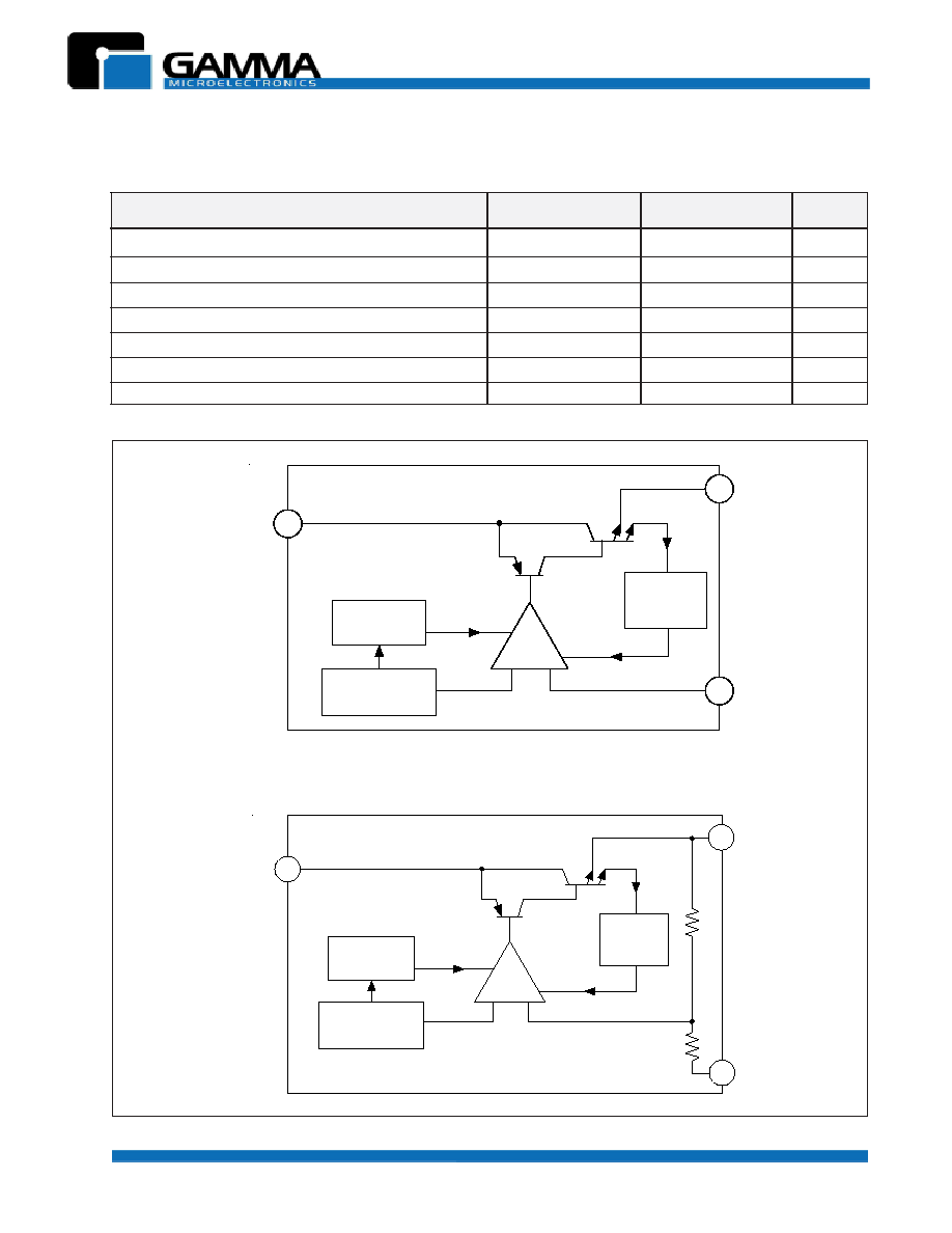
CONNECTION DIAGRAMS
Applications:
Microprocessor Supply
Post Regulators for Switching Supplies
Telecommunication Systems
Printer Supplies
Motherboards
V
OUT
GND
V
IN
3.3V @ 3.0A
10
µ
F
5.0V
100
µ
F
5.0V
5.0V
GM6603-3.3
TYPICAL APPLICATION CIRCUITS
(Fixed Version)
(
Adjustable
Version)
V
OUT
ADJ
V
IN
3.3V @ 3.0A
22
µ
F
5.0V
10
µ
F
5.0V
GM6603-A
5.0V
0.1
µ
F
5.0V
Tant
200
1.0%
124
1.0%
TO-252 (D-PAK)
3
VIN
2
VOUT
1
ADJ / GND*
3
2
1
VIN
VOUT
ADJ / GND*
TO-220 3-LEAD
VIN
VOUT
ADJ/GND*
TO-263 (D2PAK)
3
2
1
(Top View)
(Top View)
* On fixed versions Pin1=GND,
on adjustable versions Pin1=ADJ
(Top View)
Revision 2, February 2003 4 www.gammamicro.com
3.0A PRECISION LINEAR REGULATORS
GM6603
PRELIMINARY
The GM6603 series linear regulators provide fixed and
adjustable output voltages at currents up to 1.5 A. These
regulators are protected against overcurrent conditions
and include thermal shutdown protection. The GM6603's
have a composite PNP≠NPN output transistor and
require an output capacitor for stability.
A detailed procedure for selecting this capacitor follows.
Stability Considerations
The output compensation capacitor helps to determine
three main characteristics of a linear regulator's
performance: start≠up delay, load transient response,
and loop stability. The capacitor value and type is based
on cost, availability, size and temperature constraints. A
tantalum or aluminum electrolytic capacitor is preferred,
as a film or ceramic capacitor with almost zero ESR
can cause instability. An aluminum electrolytic capacitor
is the least expensive type, but when the circuit operates
at low temperatures, both the value and ESR of the
capacitor will vary widely. For optimum performance over
the full operating temperature range, a tantalum
capacitor is best. A 22
µ
F tantalum capacitor will work
fine in most applications, but with high current regulators
such as the GM6603 higher capacitance values will
improve the transient response and stability. Most
applications for the GM6603's involve large changes in
load current, so the output capacitor must supply
instantaneous load current. The ESR of the output
capacitor causes an immediate drop in output voltage
given by:
In microprocessor applications an output capacitor
network of several tantalum and ceramic capacitors in
parallel is commonly used. This reduces overall ESR
and minimizes the instantaneous output voltage drop
under transient load conditions. The output capacitor
network should be placed as close to the load as
possible for the best results.
V =
I x ESR
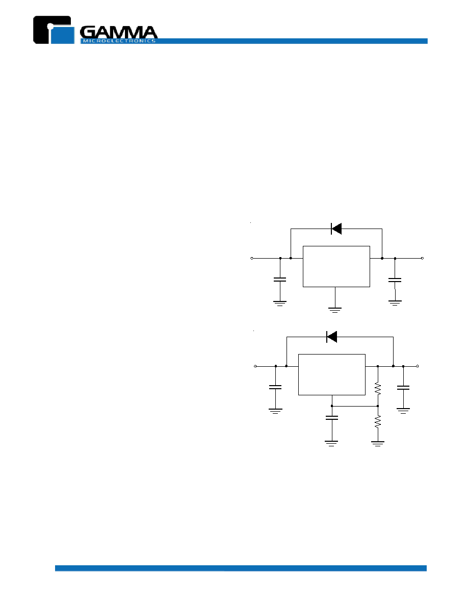
Protection Diodes
When large external capacitors are used with most linear
regulator it is wise to add protection diodes. If the input
voltage of the regulator is shorted, the output capacitor
will discharge into the output of the regulator. The
discharge current depends on the value of capacitor,
output voltage and rate at which V
IN
drops.
In the GM6603 linear regulators, the discharge path is
through a large junction, and protection diodes are
normally not needed. However, if the regulator is used
with large output capacitance values and the input
voltage is instantaneously shorted to ground, damage
can occur. In this case, a diode connected as shown
above in Figure 1.
V
OUT
GND
V
IN
GM6603-3.3
V
OUT
V
IN
C1
C2
IN4002
V
OUT
ADJ
V
IN
GM6603-A
V
OUT
V
IN
C1
C2
IN4002
R1
R2
C
ADJ
(a) Fixed Version
(b) Adjustable Version
FIGURE 1
(a),(b)
Protection Diode Scheme for
Large Output Capacitors
APPLICATIONS INFORMATION
Revision 2, February 2003 5 www.gammamicro.com
3.0A PRECISION LINEAR REGULATORS
GM6603
PRELIMINARY
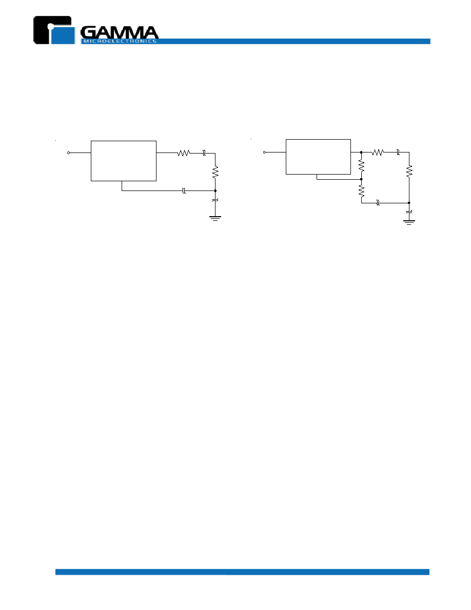
Output Voltage Sensing
The GM6603 series are three terminal regulators, so they cannot provide true remote load sensing. Load regulation
is limited by the resistance of the conductors connecting the regulator to the load. For best results the GM6603
should be connected as shown in Figure 2.
V
OUT
V
IN
GM6603-3.3
V
IN
R
C
R
LOAD
GND
FIGURE 2
(a),(b)
Conductor Parasitic Resistance Effects are Minimized by this
Grounding Scheme For Fixed and Adjustable Output Regulators
(a) Fixed Version
(b) Adjustable Version
V
OUT
V
IN
GM6603-A
V
IN
R
C
R
LOAD
ADJ
R
2
R
1
Conductor
Parasitic
Resistance
Calculating Power Dissipation and Heat Sink Requirements
The GM6603 series precision linear regulators include thermal shutdown and current limit circuitry to protect the
devices. However, high power regulators normally operate at high junction temperatures so it is important to
calculate the power dissipation and junction temperatures accurately to be sure that you use and adequate heat
sink. The case is connected to V
OUT
on the GM6603, so electrical isolation may be required for some applications.
Thermal compound should always be used with high current regulators like the GM6603.
The thermal characteristics of an IC depend four factors:
1.Maximum Ambient Temperature T
A
(∞C)
2.Power Dissipation P
D
(Watts)
3.Maximum Junction Temperature T
J
(∞C)
4.Thermal Resistance Junction to ambient R
JA
(∞C/W)
These relationship of these four factors is expressed
by equation (1):
T
J
= T
A
+ P
D
x R
JA
Conductor
Parasitic
Resistance
Maximum ambient temperature and power dissipation
are determined by the design while the maximum
junction temperature and thermal resistance depend on
the manufacturer and the package type.
The maximum power dissipation for a regulator is
expressed by equation (2):
P
D(max)
={V
IN(max)
-V
OUT(min)
}I
OUT(max)
+V
IN(max)
I
Q
where:
V
IN(max)
is the maximum input voltage,
V
OUT(min)
is the minimum output voltage,
I
OUT(max)
is the maximum output current
I
Q
is the maximum quiescent current at I
OUT(max)
.
A heat sink effectively increases the surface area of
the package to improve the flow of heat away from
the IC into the air. Each material in the heat flow path
between the IC and the environment has a thermal
resistance. Like series electrical resistances, these
resistances are summed to determine R
JA,
the total
thermal resistance between the junction and the air.
This is expressed by equation (3):
where all of the following are in ∞C/W:
R
JC
is thermal resistance of junction to case,
R
CS
is thermal resistance of case to heat sink,
R
SA
is thermal resistance of heat sink to ambient air
R
JA
= R
JC
+
R
CS
+ R
SA
The value for R
JA
is calculated using equation (3)
and the result can be substituted in equation (1). The
value for R
JC
is 3.5∞C/W for a given package type
based on an average die size. For a high current
regulator such as the GM6603 the majority of the heat
is generated in the power transistor section.