Revision 2, December 2002 www.gammamicro.com
1A LOW-DROPOUT VOLTAGE REGULATORS
GM66102
PRELIMINARY
1
Fixed and Adjustable Voltage Versions
Output Current up to 1A
Low Dropout Voltage 350mV @ 1A
Low Ground Current
Accurate 1% Guaranteed Tolerance
Extremely Fast Transient Response
Reverse-battery Protection
"Load Dump" Protection
The GM66102 series of positive fixed and adjustable regulators are designed to provide up to 1A output with
high current, high accuracy and extremely low dropout voltage performance. These regulators feature 300 to
350mV (full load) dropout voltages and very low ground current. Although designed for high current loads,
these devices are also useful in lower current, extremely low dropout-critical systems, where their minimal
dropout voltage and ground current values are important characteristics.
The GM66102's are fully protected against overcurrent, reversed input polarity (or reversed battery connection),
reversed lead insertion, over-temperature operation, and transient voltage spikes (positive or negative).
The GM66102's are available in TO-220, SOT-223, TO-252 and TO-263 packages.
PIN CONFIGURATIONS
Applications:
High Efficiency Linear Regulators
Post Regulators for Switching Supplies
Battery Powered Equipment
Automotive Electronics
3
2
1
TO-220 3-LEAD
GND
V
IN
V
OUT
GND
V
IN
TO-263 (D2PAK)
V
OUT
3
2
1
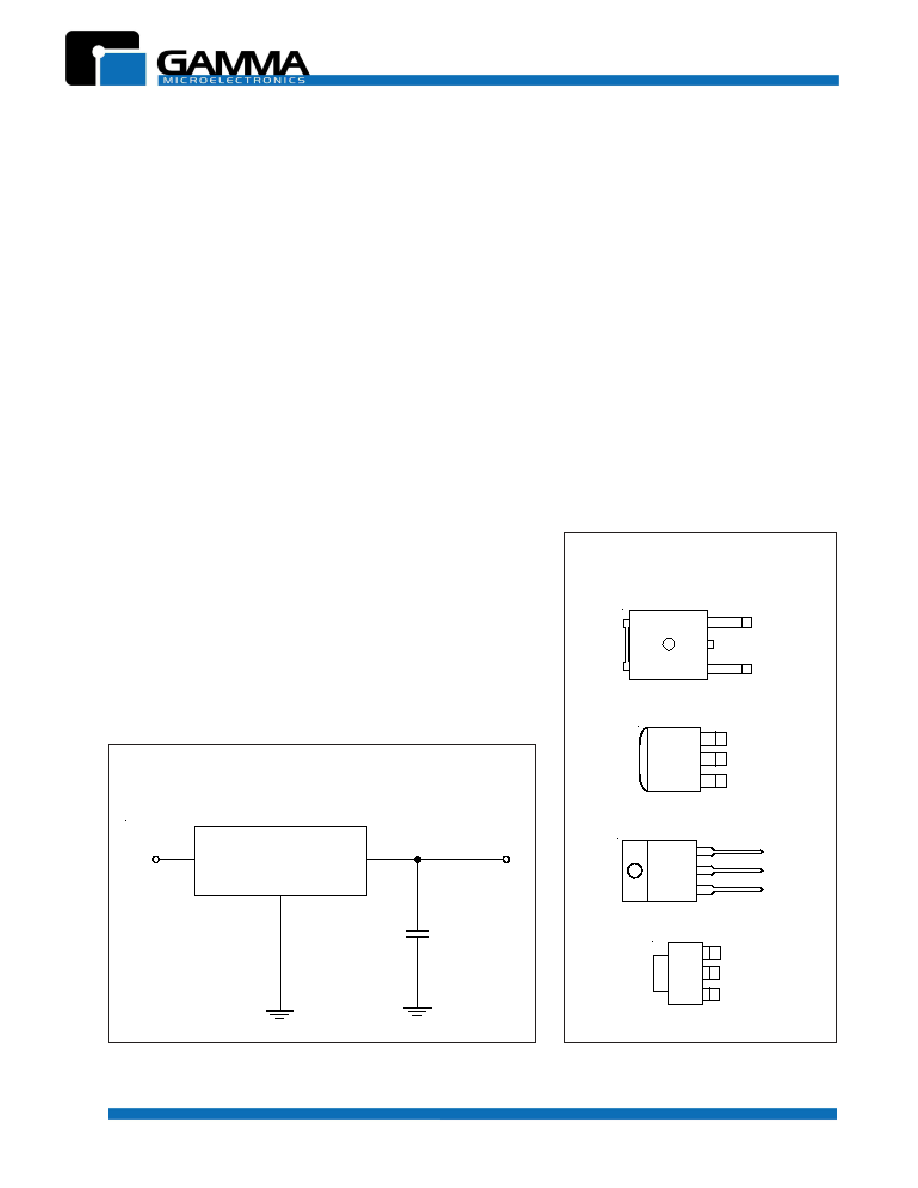
TYPICAL APPLICATION CIRCUIT
GM66102-3.3
5V�5%
3.3V�1%
@ 1A
33
�
F
+
TAB is GND
TO-252 (D-PAK)
3
2
1
V
IN
V
OUT
(Top View)
3
2
1
VIN
VOUT
GND
SOT-223
Revision 2, December 2002 www.gammamicro.com
1A LOW-DROPOUT VOLTAGE REGULATORS
GM66102
PRELIMINARY
2
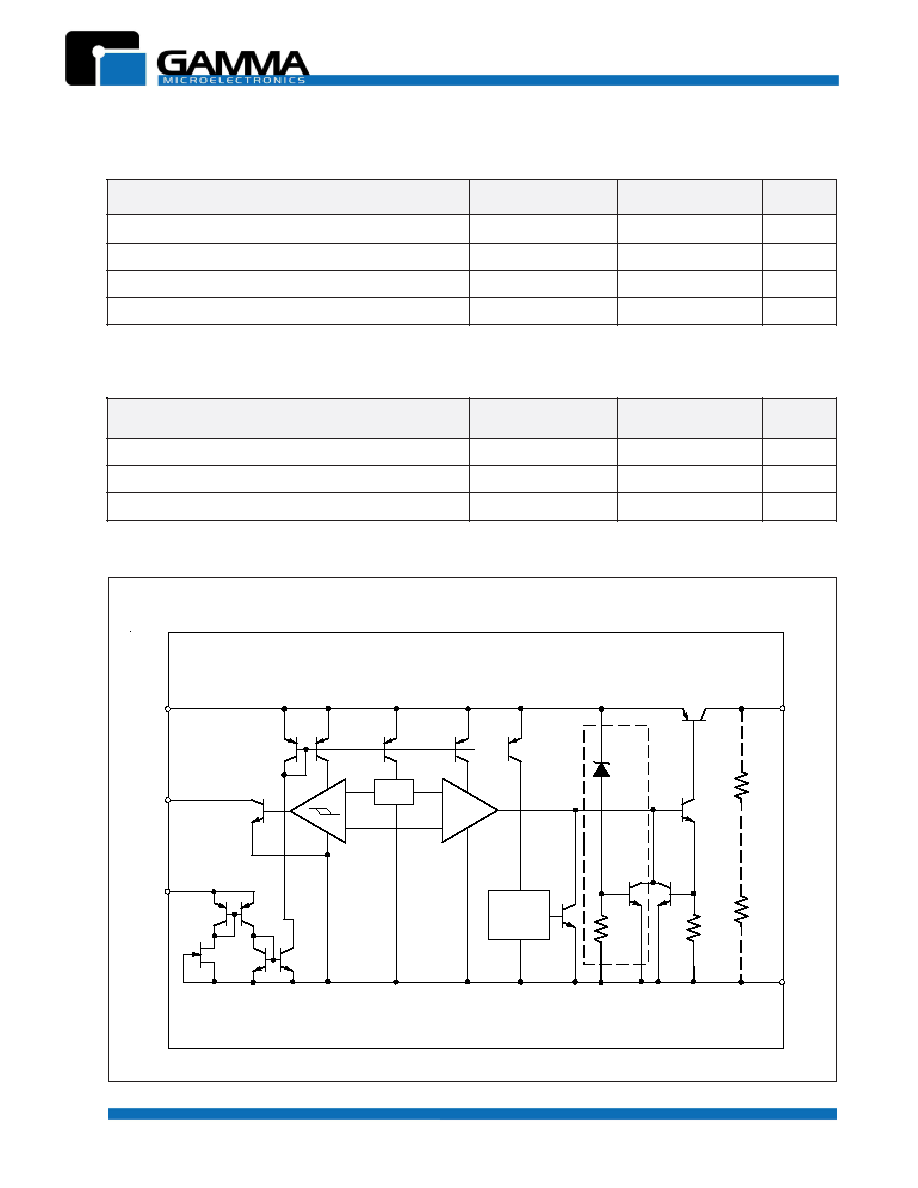
BLOCK DIAGRAM
r
e
t
e
m
a
r
a
P
l
o
b
m
y
S
e
u
l
a
V
t
i
n
U
r
e
w
o
P
n
o
it
a
p
i
s
s
i
D
P
D
d
e
ti
m
il
y
ll
a
n
r
e
t
n
I
W
e
g
a
tl
o
V
y
l
p
p
u
S
t
u
p
n
I
V
N
I
0
6
+
o
t
0
2
-
V
)
c
e
s
5
,
g
n
ir
e
d
l
o
S
(
e
r
u
t
a
r
e
p
m
e
T
d
a
e
L
T
D
A
E
L
0
6
2
C
�
e
g
n
a
R
e
r
u
t
a
r
e
p
m
e
T
e
g
a
r
o
t
S
T
G
T
S
0
5
1
+
o
t
5
6
�
C
�
r
e
t
e
m
a
r
a
P
l
o
b
m
y
S
e
u
l
a
V
t
i
n
U
e
g
a
tl
o
V
t
u
p
n
I
g
n
it
a
r
e
p
O
m
u
m
i
x
a
M
V
N
I
6
2
V
e
g
n
a
R
e
r
u
t
a
r
e
p
m
e
T
n
o
it
c
n
u
J
g
n
it
a
r
e
p
O
T
J
5
2
1
+
o
t
0
4
�
C
�
e
c
n
a
t
s
i
s
e
R
l
a
m
r
e
h
T
C
J
0
.
2
W
/
C
�
OPERATING RATINGS
ABSOLUTE MAXIMUM
RATINGS
IN
FLAG
Ref.
+
-
+
-
1.18V
1.24V
EN
GND
OUT
28V
R1
R2
Revision 2, December 2002 www.gammamicro.com
1A LOW-DROPOUT VOLTAGE REGULATORS
GM66102
PRELIMINARY
3
Unless otherwise specified:
T
J
= 25
�
C; Bold values are guaranteed across the operating temperature range.
(Note1)
S
C
I
T
S
I
R
E
T
C
A
R
A
H
C
S
N
O
I
T
I
D
N
O
C
T
S
E
T
N
I
M
P
Y
T
X
A
M
T
I
N
U
e
g
a
tl
o
V
t
u
p
t
u
O
)
2
e
t
o
N
(
I
O
A
m
0
1
=
1
-
1
%
A
m
0
1
I
O
I
L
F
(
, V
T
U
O
)
V
1
+
V
N
I
V
6
2
2
-
2
%
n
o
it
a
l
u
g
e
R
e
n
i
L
I
O
,
A
m
0
1
=
(V
T
U
O
)
V
1
+
V
N
I
V
6
2
6
0
.
0
5
.
0
%
n
o
it
a
l
u
g
e
R
d
a
o
L
V
N
I
V
=
T
U
O
,
V
5
+
A
m
0
1
I
T
U
O
I
L
F
0
2
.
0
0
.
1
%
e
r
u
t
a
r
e
p
m
e
T
h
ti
w
e
g
n
a
h
c
e
g
a
tl
o
V
t
u
p
t
u
O
)
6
e
t
o
N
(
.f
e
o
C
V
T
U
O
/
T
0
2
0
0
1
C
�
/
m
p
p
e
g
a
tl
o
V
t
u
o
p
o
r
D
V
T
U
O
)
3
e
t
o
N
(
%
1
-
=
I
O
A
m
0
0
1
=
I
O
A
m
0
5
7
=
I
O
A
0
.
1
=
0
8
0
2
2
0
5
3
0
0
2
0
0
6
V
m
t
n
e
r
r
u
C
d
n
u
o
r
G
I
O
V
,
A
m
0
5
7
=
N
I
V
=
T
U
O
V
1
+
I
O
A
0
.
1
=
8
2
2
0
2
A
m
t
u
o
p
o
r
D
t
a
t
n
e
r
r
u
C
n
i
P
d
n
u
o
r
G
I
O
D
D
N
G
V
N
I
V
d
e
if
i
c
e
p
s
n
a
h
t
s
s
e
l
V
5
.
0
=
T
U
O
,
I
T
U
O
)
5
e
t
o
N
(
,
A
m
0
1
=
9
.
0
A
m
ti
m
i
L
t
n
e
r
r
u
C
V
T
U
O
)
4
e
t
o
N
(
V
0
=
1
.
2
5
.
3
A
e
e
g
a
tl
o
V
e
s
i
o
N
t
u
p
t
u
O
n
)
z
H
k
0
0
1
o
t
z
H
0
1
(
,
I
O
A
m
0
0
1
=
C
L
0
1
=
�
F
C
L
3
3
=
�
F
0
0
4
0
6
2
�
V
)
s
m
r
(
ELECTRICAL CHARACTERISTICS
Notes:
Note 1: Maximum positive supply voltage of 60V must be of limited duration (<100msec) and duty cycle (
1%).
The maximum continuous supply voltage is 26V.
Note 2: Full Load current (I
FL
) is defined as 1.0A for the GM66102 series.
Note 3: Dropout voltage is defined as the input-to-output differential when the output voltage drops to 99% of its
nominal value with V
OUT
+ 1V applied to V
IN
Note 4: V
IN
= V
OUT
(nominal) + 1V. For example, use V
IN
= 4.3V for a 3.3V regulator or use 6V for a 5V regulator.
Employ pulse-testing procedures to minimize temperature rise.
Note 5: Ground pin current is the regulator quiescent current. The total current drawn from the source is the sum of the
load current plus the ground pin current.
Note 6: Output voltage temperature coefficient is defined as the worst case voltage change divided by the total
temperature range.
Revision 2, December 2002 www.gammamicro.com
1A LOW-DROPOUT VOLTAGE REGULATORS
GM66102
PRELIMINARY
4
The GM66102 series are high performance, low-
dropout voltage regulators suitable for all moderate
to high-current voltage regulator applications. Their
350mV dropout voltage at full load make them
especially valuable in battery powered systems and
as high efficiency noise filters in "post-regulator"
applications. Unlike older NPN-pass transistor
designs, where the minimum dropout voltage is limited
by the base-emitter voltage drop and collector-emitter
saturation voltage, dropout performance of the PNP
output of these devices is limited merely by the low
V
CE
saturation voltage. A trade-off for the low dropout
voltage is a varying base drive requirement.But
Gamma's PNP process reduces this drive requirement
to merely 1% of the load current.
The GM66102 series of regulators are fully protected
from damage due to fault conditions. Current limiting
is provided. This limiting is linear; output current under
overload conditions is constant.
Thermal shutdown disables the device when the die
temperature exceeds the 125
�
C maximum safe
operating temperature. Transient protection allows
device (and load) survival even when the input voltage
spikes between �20V and +60V. When the input
voltage exceeds about 35V to 40V, the overvoltage
sensor temporarily disables the regulator. The output
structure of these regulators allows voltages in excess
of the desired output voltage to be applied without
reverse current flow.
An additional feature of this regulator family is a
common pinout: a design's current requirement may
change up or down yet use the same board layout,
as all of these regulators have identical pinouts.
+
+
GND
OUT
IN
V
IN
V
OUT
Figure 3. Linear regulators require only two
capacitors for operation.
Thermal Design
Linear regulators are simple to use. The most
complicated design parameters to consider are
thermal characteristics. Thermal design requires the
following application-specific parameters:
� Maximum ambient temperature, T
A
� Output Current, I
OUT
� Output Voltage, V
OUT
� Input Voltage, V
IN
First, we calculate the power dissipation of the
regulator from these numbers and the device
parameters from this formula:
P
D
= I
OUT
( 1.01V
IN
- V
OUT
)
where the ground current is approximated by 1% of
I
OUT
.
Then the heat sink thermal resistance is determined
with this formula:
SA
= (
JC
+
CS
)
T
J(MAX)
- T
A
P
D
where T
J(MAX)
125
�
C and
CS
is between 0 and
2
�
C/W.
The heat sink may be significantly reduced in
applications where the minimum input voltage is
known and is large compared with the dropout
voltage. Use a series input resistor to drop excessive
voltage and distribute the heat between this resistor
and the regulator. The low dropout properties of
Gamma PNP regulators allow very significant
reductions in regulator power dissipation and the
associated heat sink without compromising
performance. When this technique is employed, a
capacitor of at least 0.1
�
F is needed directly between
the input and regulator ground.
APPLICATIONS
INFORMATION
Revision 2, December 2002 www.gammamicro.com
1A LOW-DROPOUT VOLTAGE REGULATORS
GM66102
PRELIMINARY
5
Capacitor Requirements
For stability and minimum output noise, a capacitor
on the regulator output is necessary. The value of
this capacitor is dependent upon the output current;
lower currents allow smaller capacitors. GM66102
regulators are stable with the minimum capacitor
value of 10
�
F at full load. This capacitor doesn't need
to be an expensive low ESR type: aluminum electro-
lytics are adequate. In fact, extremely low ESR capa-
citors may contribute to instability. Tantalum capacitors
are recommended for systems where fast load
transient response is important.
Minimum Load Current
The GM66102 regulators are specified between finite
loads. If the output current is too small, leakage
currents dominate and the output voltage rises. The
5mA minimum load current swamps any expected
leakage current across operating temperature range.
Where the regulator is powered from a source with a
high AC impedance, a 0.1
�
F capacitor connected
between Input and GND is recommended. This
capacitor should have good characteristics to above
250kHz.
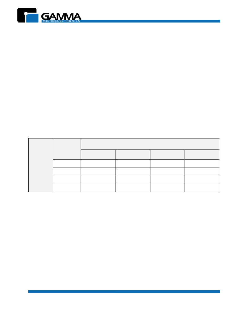
2
0
1
6
6
M
G
E
G
A
K
C
A
P
e
g
a
tl
o
V
t
u
p
t
u
O
V
5
.
1
V
5
.
2
V
0
.
3
V
3
.
3
3
6
2
-
O
T
3
A
T
5
.
1
-
2
0
1
6
6
M
G
3
A
T
5
.
2
-
2
0
1
6
6
M
G
3
A
T
0
.
3
-
2
0
1
6
6
M
G
3
A
T
3
.
3
-
2
0
1
6
6
M
G
0
2
2
-
O
T
3
B
T
5
.
1
-
2
0
1
6
6
M
G
3
B
T
5
.
2
-
2
0
1
6
6
M
G
3
B
T
0
.
3
-
2
0
1
6
6
M
G
3
B
T
3
.
3
-
2
0
1
6
6
M
G
3
2
2
-
T
O
S
3
T
S
5
.
1
-
2
0
1
6
6
M
G
3
T
S
5
.
2
-
2
0
1
6
6
M
G
3
T
S
0
.
3
-
2
0
1
6
6
M
G
3
T
S
3
.
3
-
2
0
1
6
6
M
G
2
5
2
-
O
T
3
C
T
5
.
1
-
2
0
1
6
6
M
G
3
C
T
5
.
2
-
2
0
1
6
6
M
G
3
C
T
0
.
3
-
2
0
1
6
6
M
G
3
C
T
3
.
3
-
2
0
1
6
6
M
G
ORDERING INFORMATION