 | –≠–ª–µ–∫—Ç—Ä–æ–Ω–Ω—ã–π –∫–æ–º–ø–æ–Ω–µ–Ω—Ç: GM7001 | –°–∫–∞—á–∞—Ç—å:  PDF PDF  ZIP ZIP |

GM7001
BIPOLAR LOW VOLTAGE SWITCHING REGULATOR CONTROLLER
Revision 1, May 2002 1 www.gammamicro.com
(TOP VIEW)
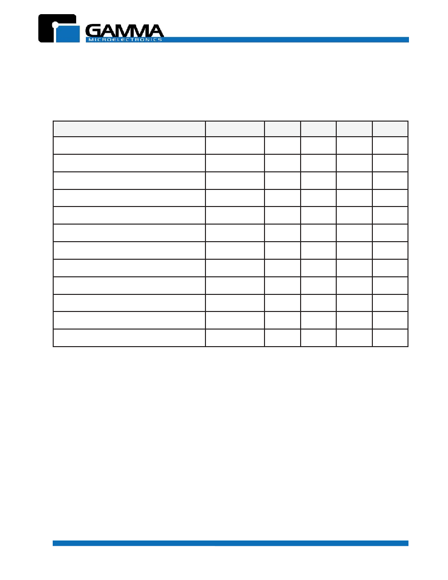
PIN ASSIGNMENT
OUT
Supply voltage operating range from 1.8 to 15 V
Low current consumption: 5.5 mA (typical) operating, 1
µµ
µµ
µ
A or less stand-by
High speed operation up to 1 MHz
Error amplifier gain is set in the chip to minimize peripheral components
Soft-start circuit on-chip
Timer-latch short-circuit detection circuit (SCP) on-chip
Totem-pole output with adjustable on/off current for NPN transistors
Stand-by function
SOP-8, SOL-8 and SSOP-8 packages available
The GM7001 is a single-channel low-voltage switching regulator control IC with soft-start function and short-circuit
detection, capable of 1MHz operation. With its low minimum operating voltage of 1.8V and minimal current
consumption, the GM7001 is ideal for power supplies in battery-operated equipment.
1
2
3
4
8
7
6
5
GND
OSC
FB
-IN
SCP
V
CC
BR/CTL
.
o
N
N
I
P
L
O
B
M
Y
S
O
/I
N
O
I
T
P
I
R
C
S
E
D
1
N
I
-
I
n
i
p
t
u
p
n
i
g
n
it
r
e
v
n
i
r
e
if
il
p
m
a
r
o
r
r
E
2
P
C
S
-
n
i
p
n
o
it
c
e
n
n
o
c
r
o
ti
c
a
p
a
c
g
n
it
t
e
s
P
C
S
d
n
a
t
r
a
t
s
tf
o
S
3
V
C
C
-
n
i
p
y
l
p
p
u
s
r
e
w
o
P
4
L
T
C
/
R
B
I
n
i
p
l
o
r
t
n
o
c
d
n
a
g
n
it
t
e
s
t
n
e
r
r
u
c
t
u
p
t
u
O
5
T
U
O
O
n
i
p
t
u
p
t
u
o
e
p
y
t
e
l
o
p
-
m
e
t
o
T
6
D
N
G
-
n
i
p
d
n
u
o
r
G
7
C
S
O
-
y
c
n
e
u
q
e
rf
n
o
it
a
ll
i
c
s
o
e
h
t
g
n
it
t
e
s
r
o
f
n
i
p
n
o
it
c
e
n
n
o
c
r
o
t
s
i
s
e
r
d
n
a
r
o
ti
c
a
p
a
C
8
B
F
O
n
i
p
t
u
p
t
u
o
r
e
if
il
p
m
a
r
o
r
r
E

GM7001
BIPOLAR LOW VOLTAGE SWITCHING REGULATOR CONTROLLER
Revision 1, May 2002 2 www.gammamicro.com
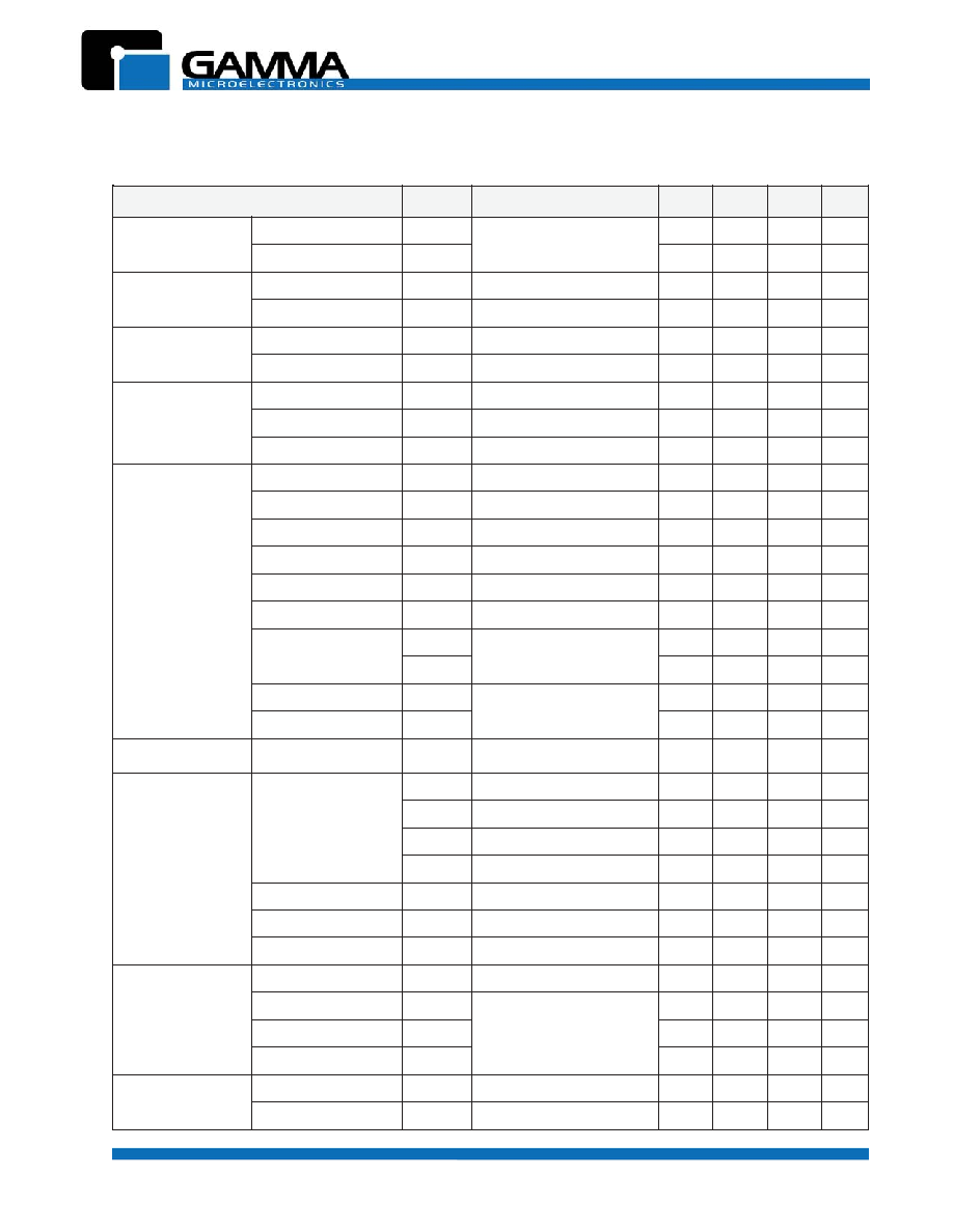
+
-
+
+
+
-
1
2
4
3
5
6
7
8
Reference
Voltage Supply
Sawtooth
Wave Oscillator
500
36 k
30 k
Output Drive
Control Circuit
Soft Start
S C P
DTC 0.6 V
1.25 V
0.3 V
PWM Comp.
0.1 V
0.5 V
Error Amp.
0.6 V≠
0.1 V≠
OUT
GND
OSC
FB
-IN
SCP
V
CC
BR/CTL
BLOCK DIAGRAM
R
E
T
E
M
A
R
A
P
L
O
B
M
Y
S
N
O
I
T
I
D
N
O
C
N
I
M
X
A
M
S
T
I
N
U
e
g
a
tl
o
V
y
l
p
p
u
S
r
e
w
o
P
V
C
C
-
-
6
1
V
t
n
e
r
r
u
C
e
c
r
u
o
S
t
u
p
t
u
O
I
O
+
-
-
0
5
-
A
m
t
n
e
r
r
u
C
k
n
i
S
t
u
p
t
u
O
I
O
-
-
-
0
5
a
m
e
l
b
a
w
o
ll
A
n
o
it
a
p
i
s
s
i
D
P
D
T
,
8
-
P
O
S
A
#
#
#
#
#
C
∞
5
2
+
-
*
0
7
5
W
m
T
,
8
-
P
O
S
A
#
#
#
#
#
C
∞
5
2
+
-
*
0
3
4
W
m
T
,
8
-
P
O
S
S
A
#
#
#
#
#
C
∞
5
2
+
-
*
0
8
5
W
m
e
r
u
t
a
r
e
p
m
e
T
g
n
it
a
r
e
p
O
T
r
p
o
-
0
3
-
5
8
+
C
∞
e
r
u
t
a
r
e
p
m
e
T
e
g
a
r
o
t
S
T
g
t
s
-
5
5
-
5
2
1
+
C
∞
ABSOLUTE MAXIMUM RATINGS
T
A
=25
∞
C
* Note: When mounted on a 10 cm square double-sided epoxy board
The devices can be permanently damaged by application of stress (voltage, current,temperature, etc.)
in excess of absolute maximum ratings. Do not exceed these ratings. Refer to Recommended Operating
Conditions, page 3.
GM7001
BIPOLAR LOW VOLTAGE SWITCHING REGULATOR CONTROLLER
Revision 1, May 2002 3 www.gammamicro.com
r
e
t
e
m
a
r
a
P
l
o
b
m
y
S
.
N
I
M
.
P
Y
T
.
X
A
M
t
i
n
U
e
g
a
tl
o
v
y
l
p
p
u
s
r
e
w
o
P
V
C
C
8
.
1
--
5
1
V
e
g
a
tl
o
v
t
u
p
n
i
r
e
if
il
p
m
a
r
o
r
r
E
V
I
2
.
0
≠
--
0
.
1
V
e
g
a
tl
o
v
t
u
p
n
i
n
i
p
L
T
C
/
R
B
V
R
B
2
.
0
≠
--
V
C
C
V
t
n
e
r
r
u
c
e
c
r
u
o
s
t
u
p
t
u
O
I
O
+
0
4
≠
--
--
A
m
t
n
e
r
r
u
c
k
n
i
s
t
u
p
t
u
O
I
O
≠
--
--
0
4
A
m
e
c
n
a
ti
c
a
p
a
c
n
i
p
P
C
S
C
E
P
--
1
.
0
--
:
F
e
c
n
a
ti
c
a
p
a
c
n
o
it
a
s
n
e
p
m
o
c
e
s
a
h
P
C
P
--
1
.
0
--
:
F
e
c
n
a
t
s
i
s
e
r
g
n
it
t
e
s
t
n
e
r
r
u
c
t
u
p
t
u
O
R
B
0
5
1
0
9
3
0
0
0
5
S
e
c
n
a
t
s
i
s
e
r
g
n
i
m
i
T
R
T
0
.
1
0
.
3
0
.
0
1
k
S
e
c
n
a
ti
c
a
p
a
c
g
n
i
m
i
T
C
T
0
0
1
0
7
2
0
0
0
0
1
F
p
y
c
n
e
u
q
e
r
f
n
o
it
a
ll
i
c
s
O
f
C
S
O
0
1
0
0
5
0
0
0
1
z
H
k
e
r
u
t
a
r
e
p
m
e
t
g
n
it
a
r
e
p
O
T
P
O
0
3
≠
5
2
+
5
8
+
C
∞
RECOMMENDED OPERATING CONDITIONS
NOTE: "Recommended operating conditions" are normal operating ranges for the device. All the device's electrical characteristics are
guaranteed when operated within these ranges. Operation outside the recommended ranges may adversely affect reliability and could
result in device failure. No warranty is made with respect to uses, operating conditions, or combinations not represented on the data
sheet.
GM7001
BIPOLAR LOW VOLTAGE SWITCHING REGULATOR CONTROLLER
Revision 1, May 2002 4 www.gammamicro.com
ELECTRICAL CHARACTERISTICS
(T
A
= 25∫ C, V
CC
=+2V)
R
E
T
E
M
A
R
A
P
L
O
B
M
Y
S
N
O
I
T
I
D
N
O
C
.
N
I
M
.
P
Y
T
.
X
A
M
T
I
N
U
t
n
e
v
e
r
p
o
t
ti
u
c
r
i
C
t
u
p
n
i
w
o
l
t
a
n
o
it
c
n
u
fl
a
m
)
.
O
.
L
.
V
.
U
(
e
g
a
tl
o
v
e
g
a
tl
o
v
t
e
s
e
R
V
R
--
--
--
9
.
0
V
e
g
a
tl
o
v
d
l
o
h
s
e
r
h
T
V
H
T
1
.
1
3
.
1
5
.
1
V
t
r
a
t
S
tf
o
S
t
n
e
r
r
u
c
g
n
i
g
r
a
h
C
I
S
C
V
P
C
S
V
0
=
5
.
1
≠
0
.
1
≠
7
.
0
≠
:
A
tl
o
V
n
o
it
e
l
p
m
o
c
t
r
a
t
s
tf
o
s
t
a
e
g
a
V
S
t
--
7
.
0
8
.
0
9
.
0
V
n
o
it
c
e
t
e
D
ti
u
c
r
i
C
t
r
o
h
S
)
P
C
S
(
t
n
e
r
r
u
c
g
n
i
g
r
a
h
C
I
C
P
C
V
P
C
S
V
0
=
5
.
1
≠
0
.
1
≠
7
.
0
≠
:
A
e
g
a
tl
o
v
d
l
o
h
s
e
r
h
T
V
C
P
t
--
7
.
0
8
.
0
9
.
0
V
r
o
t
a
ll
i
c
s
O
e
v
a
W
h
t
o
o
t
w
a
S
)
C
S
O
(
y
c
n
e
u
q
e
r
f
n
o
it
a
ll
i
c
s
O
f
S
C
O
R
T
0
.
3
=
k
S
C
,
T
F
p
0
7
2
=
0
0
4
0
0
5
0
0
6
z
H
k
y
ti
li
b
a
t
s
t
u
p
n
i
y
c
n
e
u
q
e
r
F
f
V
d
V
C
C
V
5
1
o
t
V
2
=
--
2
0
1
%
n
o
it
a
ir
a
v
y
c
n
e
u
q
e
r
F
w
p
m
e
t
h
ti
.
f
T
d
T
A
C
∞
5
8
+
o
t
C
∞
0
3
≠
=
--
5
--
%
r
e
if
il
p
m
A
r
o
r
r
E
e
g
a
tl
o
v
d
l
o
h
s
e
r
h
t
t
u
p
n
I
V
T
V
B
F
V
m
0
5
4
=
0
8
4
0
0
5
0
2
5
V
m
y
ti
li
b
a
t
s
t
u
p
n
i
T
V
V
V
d
T
V
C
C
V
5
1
o
t
V
2
=
--
5
0
2
V
m
.
p
m
e
t
h
ti
w
n
o
it
a
ir
a
v
T
V
V
T
d
T
T
A
C
∞
5
8
+
o
t
C
∞
0
3
≠
=
--
1
--
%
t
n
e
r
r
u
c
s
a
i
b
t
u
p
n
I
I
B
V
N
I
V
0
=
0
.
1
≠
2
.
0
≠
0
.
1
:
A
n
i
a
g
e
g
a
tl
o
V
A
V
--
0
7
0
0
1
5
4
1
V
/
V
h
t
d
i
w
d
n
a
b
y
c
n
e
u
q
e
r
F
W
B
A
V
B
d
0
=
--
6
--
z
H
M
t
u
p
t
u
o
m
u
m
i
x
a
M
e
g
n
a
r
e
g
a
tl
o
v
V
M
O
+
--
8
7
.
0
7
8
.
0
--
V
V
M
O
≠
--
5
0
.
0
2
.
0
V
t
n
e
r
r
u
c
e
c
r
u
o
s
t
u
p
t
u
O
I
M
O
+
V
B
F
V
5
4
.
0
=
--
0
4
≠
4
2
≠
:
A
t
n
e
r
r
u
c
k
n
i
s
t
u
p
t
u
O
I
M
O
≠
4
2
0
4
--
:
A
d
o
ir
e
P
e
l
d
I
n
o
it
c
e
S
t
n
e
m
t
s
u
j
d
A
e
l
c
y
c
y
t
u
d
m
u
m
i
x
a
M
t
Y
T
U
D
R
T
0
.
3
=
k
S
C
,
T
V
,
F
p
0
7
2
=
B
F
V
8
.
0
=
5
6
5
7
5
8
%
n
o
it
c
e
S
t
u
p
t
u
O
e
g
a
tl
o
v
t
u
p
t
u
O
V
1
H
O
R
B
0
9
3
=
S
I
,
O
A
m
5
1
≠
=
0
.
1
2
.
1
--
V
V
2
H
O
R
B
0
5
7
=
S
V
,
C
C
I
,
V
8
.
1
=
O
A
m
0
1
≠
=
8
.
0
0
.
1
--
V
V
1
L
O
R
B
0
9
3
=
S
I
,
O
A
m
5
1
=
--
1
.
0
2
.
0
V
V
2
L
O
R
B
0
5
7
=
S
V
,
C
C
8
.
1
=
,
V I
O
A
m
0
1
=
--
1
.
0
2
.
0
V
t
n
e
r
r
u
c
e
c
r
u
o
s
t
u
p
t
u
O
I
O
+
R
B
0
9
3
=
S
V
,
O
V
9
.
0
=
--
0
3
≠
0
2
≠
A
m
t
n
e
r
r
u
c
k
n
i
s
t
u
p
t
u
O
I
O
≠
R
B
0
9
3
=
S
V
,
O
V
3
.
0
=
0
3
0
6
--
A
m
e
c
n
a
t
s
i
s
e
r
n
w
o
d
ll
u
P
R
O
--
0
2
0
3
0
4
k
S
g
n
it
t
e
S
t
n
e
r
r
u
C
t
u
p
t
u
O
n
o
it
c
e
S
l
o
r
t
n
o
C
/
n
o
it
c
e
S
e
g
a
tl
o
v
n
i
P
V
R
B
R
B
0
9
3
=
S
2
.
0
3
.
0
4
.
0
V
n
o
it
i
d
n
o
c
ff
o
t
u
p
n
I
I
F
F
O
--
0
2
≠
--
0
:
A
n
o
it
i
d
n
o
c
n
o
t
u
p
n
I
I
N
O
--
--
5
4
≠
:
A
e
g
n
a
r
t
n
e
r
r
u
c
n
i
P
I
R
B
8
.
1
≠
--
1
.
0
≠
A
m
e
c
i
v
e
D
e
r
it
n
E
t
n
e
r
r
u
c
y
b
-
d
n
a
t
S
I
S
C
C
V
r
o
n
e
p
o
n
i
p
L
T
C
/
R
B
C
C
--
--
1
:
A
t
n
e
r
r
u
c
y
l
p
p
u
s
e
g
a
r
e
v
A
I
C
C
R
B
0
9
3
=
S
--
5
.
5
3
.
9
A
m
GM7001
BIPOLAR LOW VOLTAGE SWITCHING REGULATOR CONTROLLER
Revision 1, May 2002 5 www.gammamicro.com
SETTING THE TIME CONSTANT FOR SOFT START AND SHORT CIRCUIT DETECTION
1. Soft Start
At power on, the capacitor C
PE
connected to the SCP pin begins charging. The PWM comparator compares the soft
start setting voltage (as a proportion of the voltage at the SCP pin) with the sawtooth waveform. This comparison
controls the ON duty of the OUT pin, causing soft start operation. Upon completion of soft start operation, the voltage
at the SCP pin remains low, the soft start setting voltage remains high, and the circuit enters into output short circuit
detection wait state.
Soft start time (The time until the output ON duty reaches approximately 50%)
t
S
[s]
0.35
◊
C
PE
[
µ
F]
2. Short Circuit Protection
If the switching regulator output suddenly drops due to load effect, the error amplifier output (FB pin) is fixed at V
OM
+
and
capacitor C
PE
begins charging. When the voltage at the SCP pin reaches approximately 0.8V, the output pin is set low
and the SCP pin remains low.
Once the protection circuit activates, operation of the circuit can be restored by resetting the power supply.
Short circuit detection time
t
PE
[s]
0.8
◊
C
PE
[
µ
F]
MEASUREMENT CIRCUIT DIAGRAM
-IN
18 k
2 k
390
10
µ
F
22
µ
H
GM7001
4
5
V
OUT
I
OUT
V
CC
(5 V)