Revision 1, May 2002 www.gammamicro.com
3A STEP-DOWN VOLTAGE REGULATORS
GM7130
PRELIMINARY
1
The GM7130 series of regulators provide all the
active functions for a step-down (buck) switching
regulator, and drive 3A load with excellent line and
load regulation. GM7130's are available in fixed
output voltages of 3.3V, 5V, 12V, 15V, and a
versatile Adjustable output version. These
regulators are simple to use and require a minimum
number of external components. Features include
internal frequency compensation and a fixed-
frequency oscillator. The GM7130 series are high-
efficiency replacements for popular three-terminal
linear regulators, requiring a smaller heatsink or
even no heatsink. The GM7130's perform well with
standard inductors from several manufacturers,
simplifying the design of switch-mode power
supplies. The GM7130 series guarantee ±4%
tolerance on output voltage within specified input
voltages and output load conditions, and ±10% on
the oscillator frequency. External shutdown is
included, with 50 µA (typical) standby current. The
output switch has cycle-by-cycle current limiting,
as well as thermal shutdown for full protection
under fault conditions.
Pre-regulator for linear regulators
High-efficiency step-down buck regulator
On-card/board switching regulators
Positive to negative converter (buck-boost)
Applications:
3.3V, 5V, 12V, 15V, Adjustable output versions
Adjustable version output voltage range
1.23V to 37V ±4% max over line and load
conditions
3A output current
Input voltage range 7V to 40V
Requires only 4 external components
High efficiency
TTL shutdown capability,
low power standby mode
Thermal shutdown, current limit protection
Uses standard inductors
52 kHz fixed frequency internal oscillator
P+ Product Enhancement tested
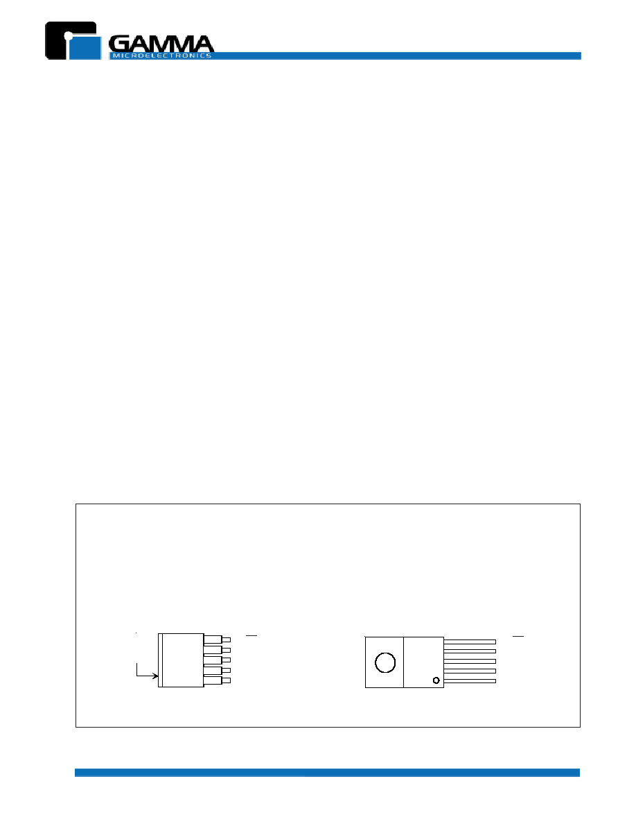
TO-263 (S)
5-Lead Surface-Mount Package
Top View
5 - ON/OFF
4 - Feedback
3 - Ground
2 - Output
1 - V
IN
TAB IS
GND
Straight Leads
5-Lead TO-220 (T)
Top View
GND
5 - ON/OFF
4 - Feedback
3 - Ground
2 - Output
1 - V
IN
Connection Diagrams
Revision 1, May 2002 www.gammamicro.com
3A STEP-DOWN VOLTAGE REGULATORS
GM7130
PRELIMINARY
1
+
5
3
L
O
A
D
+
D1
L1
4
2
Absolute Maximum Ratings
2
g
n
i
t
a
R
e
u
l
a
V
t
i
n
U
e
g
a
tl
o
V
y
l
p
p
u
S
m
u
m
i
x
a
M
5
4
V
e
g
a
tl
o
V
t
u
p
n
I
n
i
P
F
F
O
/
N
O
3
.
0
≠
#V # V
N
I
V
)
e
t
a
t
S
y
d
a
e
t
S
(
d
n
u
o
r
G
o
t
e
g
a
tl
o
V
t
u
p
t
u
O
0
.
1
-
V
n
o
it
a
p
i
s
s
i
D
r
e
w
o
P
d
e
ti
m
i
L
y
ll
a
n
r
e
t
n
I
-
e
g
n
a
R
e
r
u
t
a
r
e
p
m
e
T
e
g
a
r
o
t
S
0
5
1
+
o
t
5
6
≠
C
∞
e
r
u
t
a
r
e
p
m
e
T
n
o
it
c
n
u
J
m
u
m
i
x
a
M
0
5
1
+
C
∞
k
5
.
1
=
R
,
F
p
0
0
1
=
C
(
g
n
it
a
R
D
S
E
m
u
m
i
n
i
M
S
)
2
V
k
)
s
d
n
o
c
e
s
0
1
,
g
n
ir
e
d
l
o
S
(
e
r
u
t
a
r
e
p
m
e
T
d
a
e
L
0
6
2
+
C
∞
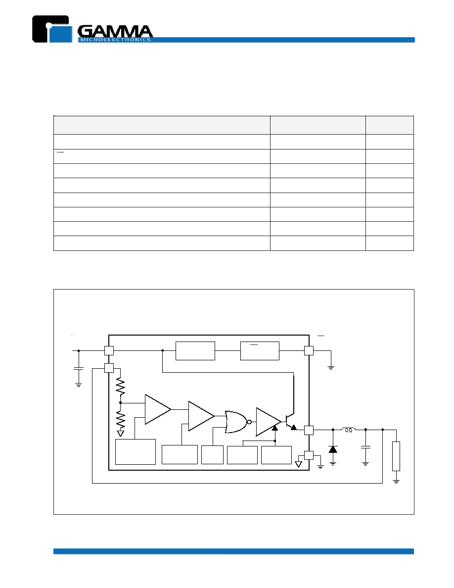
BLOCK DIAGRAM
Unregulated
DC Input
Feed-
back
V
IN
Output
C
IN
C
OUT
GND
ON/OFF
3 AMP
Switch
ON/OFF
Driver
+
Internal
Regulator
+
-
-
Fixed Gain
Error AMP
1.23V
Band - Gap
Reference
52 kHz
Oscillator
Reset
Thermal
Shutdown
Current
Limit
Comparator
Revision 1, May 2002 www.gammamicro.com
3A STEP-DOWN VOLTAGE REGULATORS
GM7130
PRELIMINARY
3
ELECTRICAL CHARACTERISTICS: GM7130-3.3
(Specifications with standard type face are for T
J
= 25∞C, and those with boldface type apply over full Operating Temperature Range)
r
e
t
e
m
a
r
a
P
s
n
o
i
t
i
d
n
o
C
l
o
b
m
y
S
n
i
M
p
y
T
x
a
M
t
i
n
U
e
g
a
tl
o
V
t
u
p
t
u
O
V
N
I
I
,
V
2
1
=
D
A
O
L
A
5
.
0
=
V
T
U
O
4
3
2
.
3
3
.
3
6
6
3
.
3
V
e
g
a
tl
o
V
t
u
p
t
u
O
V
6
# V
N
I
#
A
5
.
0
,
V
0
4
# I
D
A
O
L
#
A
0
.
3
V
T
U
O
/
8
6
1
.
3
5
3
1
.
3
3
.
3
/
2
3
4
.
3
5
6
4
.
3
V
y
c
n
e
i
c
if
f
E
V
N
I
I
,
V
2
1
=
D
A
O
L
A
0
.
3
=
0
-
5
7
-
%
ELECTRICAL CHARACTERISTICS: GM7130-5.0
(Specifications with standard type face are for T
J
= 25∞C, and those with boldface type apply over full Operating Temperature Range)
r
e
t
e
m
a
r
a
P
s
n
o
i
t
i
d
n
o
C
l
o
b
m
y
S
n
i
M
p
y
T
x
a
M
t
i
n
U
e
g
a
tl
o
V
t
u
p
t
u
O
V
N
I
I
,
V
2
1
=
D
A
O
L
A
5
.
0
=
V
T
U
O
0
0
9
.
4
0
.
5
0
0
1
.
5
V
e
g
a
tl
o
V
t
u
p
t
u
O
V
8
# V
N
I
#
A
5
.
0
,
V
0
4
# I
D
A
O
L
#
A
0
.
3
V
T
U
O
/
0
0
8
.
4
0
5
7
.
4
0
.
5
/
0
0
2
.
5
0
5
2
.
5
V
y
c
n
e
i
c
if
f
E
V
N
I
I
,
V
2
1
=
D
A
O
L
A
0
.
3
=
0
-
7
7
-
%
ELECTRICAL CHARACTERISTICS: GM7130-12
(Specifications with standard type face are for T
J
= 25∞C, and those with boldface type apply over full Operating Temperature Range)
r
e
t
e
m
a
r
a
P
s
n
o
i
t
i
d
n
o
C
l
o
b
m
y
S
n
i
M
p
y
T
x
a
M
t
i
n
U
e
g
a
tl
o
V
t
u
p
t
u
O
V
N
I
I
,
V
5
2
=
D
A
O
L
A
5
.
0
=
V
T
U
O
6
7
.
1
1
0
.
2
1
4
2
.
2
1
V
e
g
a
tl
o
V
t
u
p
t
u
O
V
5
1
# V
N
I
#
A
5
.
0
,
V
0
4
# I
D
A
O
L
#
A
0
.
3
V
T
U
O
/
2
5
.
1
1
0
4
.
1
1
0
.
2
1
/
8
4
.
2
1
0
6
.
2
1
V
y
c
n
e
i
c
if
f
E
V
N
I
I
,
V
5
1
=
D
A
O
L
A
0
.
3
=
0
-
8
8
-
%
ELECTRICAL CHARACTERISTICS: GM7130-15
(Specifications with standard type face are for T
J
= 25∞C, and those with boldface type apply over full Operating Temperature Range)
r
e
t
e
m
a
r
a
P
s
n
o
i
t
i
d
n
o
C
l
o
b
m
y
S
n
i
M
p
y
T
x
a
M
t
i
n
U
e
g
a
tl
o
V
t
u
p
t
u
O
V
N
I
I
,
V
5
2
=
D
A
O
L
A
5
.
0
=
V
T
U
O
0
7
.
4
1
0
.
5
1
0
3
.
5
1
V
e
g
a
tl
o
V
t
u
p
t
u
O
V
8
1
# V
N
I
#
A
5
.
0
,
V
0
4
# I
D
A
O
L
#
A
0
.
3
V
T
U
O
/
0
4
.
4
1
5
2
.
4
1
0
.
5
1
/
0
6
.
5
1
5
7
.
5
1
V
y
c
n
e
i
c
if
f
E
V
N
I
I
,
V
8
1
=
D
A
O
L
A
0
.
3
=
0
-
8
8
-
%
Revision 1, May 2002 www.gammamicro.com
3A STEP-DOWN VOLTAGE REGULATORS
GM7130
PRELIMINARY
4
ELECTRICAL CHARACTERISTICS: GM7130-ADJ
(Specifications with standard type face are for T
J
= 25∞C, and those with boldface type apply over full Operating Temperature Range)
r
e
t
e
m
a
r
a
P
s
n
o
i
t
i
d
n
o
C
l
o
b
m
y
S
n
i
M
p
y
T
x
a
M
t
i
n
U
e
g
a
tl
o
V
k
c
a
b
d
e
e
F
V
N
I
I
,
V
2
1
=
D
A
O
L
V
,
A
5
.
0
=
T
U
O
V
5
=
V
T
U
O
7
1
2
.
1
0
3
2
.
1
3
4
2
.
1
V
e
g
a
tl
o
V
k
c
a
b
d
e
e
F
V
8
1
# V
N
I
#
A
5
.
0
,
V
0
4
# I
D
A
O
L
#
A
0
.
3
V
T
U
O
V
5
=
V
T
U
O
/
3
9
1
.
1
0
8
1
.
1
0
3
2
.
1
/
7
6
2
.
1
0
8
2
.
1
V
y
c
n
e
i
c
if
f
E
V
N
I
I
,
V
2
1
=
D
A
O
L
V
,
A
3
=
T
U
O
V
5
=
0
-
7
7
-
%
ELECTRICAL CHARACTERISTICS: All Output Voltage Versions
(Specifications with standard type face are for T
J
= 25∞C, and those with boldface type apply over full Operating Temperature
Range. Unless otherwise specified, V
IN
= 12V for the 3.3V, 5.0V and ADJ version, V
IN
= 25V for 12V version, and V
IN
= 30V for
15V version. I
LOAD
= 500 mA)
r
e
t
e
m
a
r
a
P
s
n
o
i
t
i
d
n
o
C
l
o
b
m
y
S
n
i
M
p
y
T
x
a
M
t
i
n
U
t
n
e
r
r
u
C
s
a
i
B
k
c
a
b
d
e
e
F
V
T
U
O
)
y
l
n
O
n
o
i
s
r
e
V
e
l
b
a
t
s
u
j
d
A
(
V
5
=
I
b
-
0
5
/
0
0
1
0
0
5
A
n
y
c
n
e
u
q
e
r
F
r
o
t
a
ll
i
c
s
O
)
1
1
e
t
o
N
(
f
O
/
7
4
2
4
2
5
/
8
5
3
6
z
H
k
e
g
a
tl
o
V
n
o
it
a
r
u
t
a
S
I
T
U
O
)
4
e
t
o
N
(
A
3
=
V
T
A
S
-
4
.
1
/
8
.
1
0
.
2
V
)
N
O
(
e
l
c
y
C
y
t
u
D
x
a
M
)
5
e
t
o
N
(
C
D
3
9
8
9
-
%
ti
m
i
L
t
n
e
r
r
u
C
)
1
1
,
4
s
e
t
o
N
(
I
L
C
/
2
.
4
5
.
3
8
.
5
/
9
.
6
5
.
7
A
t
n
e
r
r
u
C
e
g
a
k
a
e
L
t
u
p
t
u
O
V
0
=
t
u
p
t
u
O
)
7
,
6
s
e
t
o
N
(
V
1
-
=
t
u
p
t
u
O
I
L
-
-
-
5
.
7
2
0
3
A
m
t
n
e
r
r
u
C
t
n
e
c
s
e
i
u
Q
)
6
e
t
o
N
(
I
Q
-
5
0
1
A
m
t
n
e
r
r
u
C
t
n
e
c
s
e
i
u
Q
y
b
d
n
a
t
S
)
F
F
O
(
V
5
=
n
i
P
F
F
O
/
N
O
I
Y
B
T
S
-
0
5
0
0
2
:
A
e
c
n
a
t
s
i
s
e
R
l
a
m
r
e
h
T
)
8
e
t
o
N
(
t
n
e
i
b
m
A
o
t
n
o
it
c
n
u
J
,
e
g
a
k
c
a
P
T
)
8
e
t
o
N
(
t
n
e
i
b
m
A
o
t
n
o
it
c
n
u
J
,
e
g
a
k
c
a
P
T
e
s
a
C
o
t
n
o
it
c
n
u
J
,
e
g
a
k
c
a
P
T
t
n
e
i
b
m
A
o
t
n
o
it
c
n
u
J
,
e
g
a
k
c
a
P
T
)
0
1
e
t
o
N
(
2
A
J
2
A
J
2
C
J
2
A
J
-
-
-
-
5
6
5
4
2
0
5
-
-
-
-
W
/
C
∞
n
i
P
F
F
O
/
N
O
l
e
v
e
L
t
u
p
n
I
c
i
g
o
L
V
T
U
O
V
0
=
V
H
I
/
2
.
2
4
.
2
4
.
1
-
V
V
T
U
O
e
g
a
tl
o
V
t
u
p
t
u
O
l
a
n
i
m
o
N
=
V
L
I
-
2
.
1
/
0
.
1
8
.
0
V
t
n
e
r
r
u
C
n
i
P
F
F
O
/
N
O
)
F
F
O
(
V
5
=
n
i
P
F
F
O
/
N
O
V
H
I
-
2
1
0
3
:
A
)
N
O
(
V
0
=
n
i
P
F
F
O
/
N
O
I
L
I
-
0
0
1
:
A

Revision 1, May 2002 www.gammamicro.com
3A STEP-DOWN VOLTAGE REGULATORS
GM7130
PRELIMINARY
5
Note 1: Absolute Maximum Ratings indicate limits beyond which damage to the device may occur. Operating Ratings
indicate conditions for which the device is intended to be functional, but do not guarantee specific performance limits.
Guaranteed specifications and test conditions are shown in Electrical Characteristics.
Note 2: All limits guaranteed at 25∞ C (standard type face) and over full operating temperature range (bold type face).
All 25∞ C limits are 100% production tested. All limits over full operating temperature range are guaranteed via
correlation using standard Statistical Quality Control methods.
Note 3: External components such as the catch diode, inductor, input and output capacitors can affect switching
regulator system performance. When the GM7130 is used as shown in the Figure 2 test circuit, system performance
will be as shown in system parameters section of Electrical Characteristics.
Note 4: Output pin sourcing current. No diode, inductor or capacitor connected to output.
Note 5: Feedback pin removed from output and connected to 0V.
Note 6: Feedback pin removed from output and connected to +12V for the Adjustable, 3.3V, and 5V versions, and
+25V for the 12V and 15V versions, to force the output transistor OFF.
Note 7: V
IN
= 40V
Note 8: Junction to ambient thermal resistance (no external heat sink) for the 5 lead TO-220 package mounted
vertically, with
Ω
inch leads in a socket, or on a PC board with minimum copper area.
Note 9: Junction to ambient thermal resistance (no external heat sink) for the 5 lead TO-220 package mounted
vertically, with
º
inch leads soldered to a PC board containing approximately 4 square inches of copper area
surrounding the leads.
Note 10: If the TO-263 package is used, the thermal resistance can be reduced by increasing the PC board copper
area thermally connected to the package. Using 0.5 square inches of copper area,
2
JA
is 50∞C/W, with 1 square inch
of copper area,
2
JA
is 37∞C/W, and with 1.6 or more square inches of copper area,
2
JA
is 32∞C/W.
Note 11: The oscillator frequency reduces to approximately 11 kHz in the event of an output short or an overload
which causes the regulated output voltage to drop approximately 40% from the nominal output voltage. This self-
protection feature lowers the average power dissipation of the GM7130 by lowering the minimum duty cycle from 5%
down to approximately 2%.
ELECTRICAL CHARACTERISTICS NOTES