
Revision 1, January 2003 www.gammamicro.com
3A STEP-DOWN VOLTAGE REGULATOR
GM7230
PRELIMINARY
1
The GM7230 series of regulators provide all the active functions for a step-down (buck) switching regulator,
and drive 3A load with excellent line and load regulation. GM7230's are available in fixed output voltages
of 3.3V, 5V, 12V, and a versatile Adjustable output version.
These regulators are simple to use and require a minimum number of external components. Features
include internal frequency compensation and a fixed-frequency oscillator. The GM7230 series are high-
efficiency replacements for popular three-terminal linear regulators, requiring a smaller heatsink or even
no heatsink.
The GM7230's perform well with standard inductors from several manufacturers, simplifying the design of
switch-mode power supplies. The GM7230 series guarantee ±4% tolerance on output voltage within
specified input voltages and output load conditions, and ±10% on the oscillator frequency.
External shutdown is included, with 80 µA (typical) standby current. The output switch has cycle-by-cycle
current limiting, as well as thermal shutdown for full protection under fault conditions.
Pre-regulator for linear regulators
High-efficiency step-down buck regulator
On-card/board switching regulators
Positive to negative converter (buck-boost)
Applications:
3.3V, 5V, 12V and Adjustable output versions
Adjustable version output voltage range 1.23V to 37V ±4% max over line and load conditions
3A output current
Input voltage range up to 40V
Requires only 4 external components
High efficiency
TTL shutdown capability, low power standby mode
Thermal shutdown, current limit protection
Uses standard inductors
150 kHz fixed frequency internal oscillator
P+ Product Enhancement tested
TO-263 (S) 5-Lead Surface-Mount Package
Top View
5 - ON/OFF
4 - Feedback
3 - Ground
2 - Output
1 - V
IN
TAB IS
GND
5-Lead TO-220 (T) - Top View
GND
5 - ON/OFF
4 - Feedback
3 - Ground
2 - Output
1 - V
IN
Connection Diagrams

Revision 1, January 2003 www.gammamicro.com
3A STEP-DOWN VOLTAGE REGULATOR
GM7230
PRELIMINARY
2
g
n
i
t
a
R
e
u
l
a
V
t
i
n
U
e
g
a
tl
o
V
y
l
p
p
u
S
m
u
m
i
x
a
M
5
4
V
e
g
a
tl
o
V
t
u
p
n
I
n
i
P
F
F
O
/
N
O
3
.
0
≠
#V # V
N
I
V
)
e
t
a
t
S
y
d
a
e
t
S
(
d
n
u
o
r
G
o
t
e
g
a
tl
o
V
t
u
p
t
u
O
0
.
1
-
V
n
o
it
a
p
i
s
s
i
D
r
e
w
o
P
d
e
ti
m
i
L
y
ll
a
n
r
e
t
n
I
-
e
g
n
a
R
e
r
u
t
a
r
e
p
m
e
T
e
g
a
r
o
t
S
0
5
1
+
o
t
5
6
≠
C
∞
e
r
u
t
a
r
e
p
m
e
T
n
o
it
c
n
u
J
m
u
m
i
x
a
M
0
5
1
+
C
∞
k
5
.
1
=
R
,
F
p
0
0
1
=
C
(
g
n
it
a
R
D
S
E
m
u
m
i
n
i
M
S
)
2
V
k
)
s
d
n
o
c
e
s
0
1
,
g
n
ir
e
d
l
o
S
(
e
r
u
t
a
r
e
p
m
e
T
d
a
e
L
0
6
2
+
C
∞
ORDERING INFORMATION
0
3
2
7
M
G
E
G
A
K
C
A
P
e
g
a
tl
o
V
t
u
p
t
u
O
.
J
D
A
V
3
.
3
V
0
.
5
V
2
1
5
-
3
6
2
-
O
T
7
M
G
2
5
A
T
A
-
0
3
7
M
G
2
5
A
T
3
.
3
-
0
3
7
M
G
2
5
A
T
0
.
5
-
0
3
7
M
G
2
5
A
T
2
1
-
0
3
5
-
0
2
2
-
O
T
7
M
G
2
5
B
T
A
-
0
3
7
M
G
2
5
B
T
3
.
3
-
0
3
7
M
G
2
5
B
T
0
.
5
-
0
3
7
M
G
2
5
B
T
2
1
-
0
3
ABSOLUTE MAXIMUM RATINGS
1
+
5
3
L
O
A
D
+
D1
L1
4
2
BLOCK DIAGRAM
Unregulated
DC Input
Feed-
back
V
IN
Output
C
IN
C
OUT
GND
ON/OFF
3 AMP
Switch
ON/OFF
Driver
+
Internal
Regulator
+
-
-
Fixed Gain
Error AMP
1.23V
Band - Gap
Reference
150 kHz
Oscillator
Reset
Thermal
Shutdown
Current
Limit
Comparator

Revision 1, January 2003 www.gammamicro.com
3A STEP-DOWN VOLTAGE REGULATOR
GM7230
PRELIMINARY
3
ELECTRICAL CHARACTERISTICS: GM7230-3.3
(Specifications with standard type face are for T
J
= 25∞C, and those with boldface type apply over full Operating Temperature Range)
ELECTRICAL CHARACTERISTICS: GM7230-5.0
(Specifications with standard type face are for T
J
= 25∞C, and those with boldface type apply over full Operating Temperature Range)
r
e
t
e
m
a
r
a
P
s
n
o
i
t
i
d
n
o
C
l
o
b
m
y
S
n
i
M
p
y
T
x
a
M
t
i
n
U
e
g
a
tl
o
V
t
u
p
t
u
O
V
N
I
I
,
V
2
1
=
D
A
O
L
A
5
.
0
=
V
T
U
O
0
0
9
.
4
0
.
5
0
0
1
.
5
V
e
g
a
tl
o
V
t
u
p
t
u
O
V
7
# V
N
I
#
A
2
.
0
,
V
0
4
# I
D
A
O
L
# A
3
V
T
U
O
/
0
0
8
.
4
0
5
7
.
4
0
.
5
/
0
0
2
.
5
0
5
2
.
5
V
y
c
n
e
i
c
if
f
E
V
N
I
I
,
V
2
1
=
D
A
O
L
A
0
.
3
=
0
-
0
8
-
%
ELECTRICAL CHARACTERISTICS: GM7230-12
(Specifications with standard type face are for T
J
= 25∞C, and those with boldface type apply over full Operating Temperature Range)
r
e
t
e
m
a
r
a
P
s
n
o
i
t
i
d
n
o
C
l
o
b
m
y
S
n
i
M
p
y
T
x
a
M
t
i
n
U
e
g
a
tl
o
V
t
u
p
t
u
O
V
N
I
I
,
V
5
2
=
D
A
O
L
A
5
.
0
=
V
T
U
O
6
7
.
1
1
0
.
2
1
4
2
.
2
1
V
e
g
a
tl
o
V
t
u
p
t
u
O
V
5
1
# V
N
I
#
A
2
.
0
,
V
0
4
# I
D
A
O
L
# A
3
V
T
U
O
/
2
5
.
1
1
0
4
.
1
1
0
.
2
1
/
8
4
.
2
1
0
6
.
2
1
V
y
c
n
e
i
c
if
f
E
V
N
I
I
,
V
5
1
=
D
A
O
L
A
0
.
3
=
0
-
0
9
-
%
r
e
t
e
m
a
r
a
P
s
n
o
i
t
i
d
n
o
C
l
o
b
m
y
S
n
i
M
p
y
T
x
a
M
t
i
n
U
e
g
a
tl
o
V
t
u
p
t
u
O
V
N
I
I
,
V
2
1
=
D
A
O
L
A
5
.
0
=
V
T
U
O
4
3
2
.
3
3
.
3
6
6
3
.
3
V
e
g
a
tl
o
V
t
u
p
t
u
O
V
5
7
.
4
# V
N
I
#
A
2
.
0
,
V
0
4
# I
D
A
O
L
# A
3
V
T
U
O
/
8
6
1
.
3
5
3
1
.
3
3
.
3
/
2
3
4
.
3
5
6
4
.
3
V
y
c
n
e
i
c
if
f
E
V
N
I
I
,
V
2
1
=
D
A
O
L
A
0
.
3
=
0
-
3
7
-
%
ELECTRICAL CHARACTERISTICS: GM7230-ADJ
(Specifications with standard type face are for T
J
= 25∞C, and those with boldface type apply over full Operating Temperature Range)
r
e
t
e
m
a
r
a
P
s
n
o
i
t
i
d
n
o
C
l
o
b
m
y
S
n
i
M
p
y
T
x
a
M
t
i
n
U
e
g
a
tl
o
V
k
c
a
b
d
e
e
F
V
N
I
I
,
V
2
1
=
D
A
O
L
V
,
A
5
.
0
=
T
U
O
V
5
=
V
T
U
O
7
1
2
.
1
0
3
2
.
1
3
4
2
.
1
V
e
g
a
tl
o
V
k
c
a
b
d
e
e
F
V
5
.
4
# V
N
I
#
A
2
.
0
,
V
0
4
# I
D
A
O
L
# A
3
V
T
U
O
V
3
=
V
T
U
O
/
3
9
1
.
1
0
8
1
.
1
0
3
2
.
1
/
7
6
2
.
1
0
8
2
.
1
V
y
c
n
e
i
c
if
f
E
V
N
I
I
,
V
2
1
=
D
A
O
L
V
,
A
3
=
T
U
O
V
5
=
0
-
3
7
-
%

Revision 1, January 2003 www.gammamicro.com
3A STEP-DOWN VOLTAGE REGULATOR
GM7230
PRELIMINARY
4
ELECTRICAL CHARACTERISTICS: All Output Voltage Versions
(Specifications with standard type face are for T
J
= 25∞C, and those with boldface type apply over full Operating Temperature Range.
Unless otherwise specified, V
IN
= 12V for the 3.3V, 5.0V and ADJ version and V
IN
= 25V for 12V version. I
LOAD
= 500 mA)
r
e
t
e
m
a
r
a
P
s
n
o
i
t
i
d
n
o
C
l
o
b
m
y
S
n
i
M
p
y
T
x
a
M
t
i
n
U
t
n
e
r
r
u
C
s
a
i
B
k
c
a
b
d
e
e
F
V
B
F
)
y
l
n
O
n
o
i
s
r
e
V
e
l
b
a
t
s
u
j
d
A
(
V
3
.
1
=
I
b
-
0
1
/
0
5
0
0
1
A
n
y
c
n
e
u
q
e
r
F
r
o
t
a
ll
i
c
s
O
)
6
e
t
o
N
(
f
O
/
7
2
1
0
1
1
0
5
1
/
3
7
1
3
7
1
z
H
k
e
g
a
tl
o
V
n
o
it
a
r
u
t
a
S
I
T
U
O
)
8
,
7
s
e
t
o
N
(
A
3
=
V
T
A
S
-
6
1
.
1
/
4
.
1
5
.
1
V
)
N
O
(
e
l
c
y
C
y
t
u
D
x
a
M
)
8
e
t
o
N
(
C
D
0
0
1
-
%
)
F
F
O
(
e
l
c
y
C
y
t
u
D
x
a
M
)
9
e
t
o
N
(
C
D
0
-
%
ti
m
i
L
t
n
e
r
r
u
C
)
8
,
7
s
e
t
o
N
(
I
L
C
/
2
.
4
5
.
3
8
.
5
/
9
.
6
5
.
7
A
t
n
e
r
r
u
C
e
g
a
k
a
e
L
t
u
p
t
u
O
V
0
=
t
u
p
t
u
O
)
0
1
,
9
,
7
s
e
t
o
N
(
V
1
-
=
t
u
p
t
u
O
I
L
-
-
-
2
0
5
0
3
A
m
t
n
e
r
r
u
C
t
n
e
c
s
e
i
u
Q
)
9
e
t
o
N
(
I
Q
-
5
0
1
A
m
t
n
e
r
r
u
C
t
n
e
c
s
e
i
u
Q
y
b
d
n
a
t
S
)
F
F
O
(
V
5
=
n
i
P
F
F
O
/
N
O
I
Y
B
T
S
-
0
8
/
0
0
2
0
5
2
:
A
e
c
n
a
t
s
i
s
e
R
l
a
m
r
e
h
T
e
s
a
C
o
t
n
o
it
c
n
u
J
,
e
g
a
k
c
a
P
T
)
1
1
e
t
o
N
(
t
n
e
i
b
m
A
o
t
n
o
it
c
n
u
J
,
e
g
a
k
c
a
P
T
)
2
1
e
t
o
N
(
t
n
e
i
b
m
A
o
t
n
o
it
c
n
u
J
,
e
g
a
k
c
a
P
T
)
3
1
e
t
o
N
(
t
n
e
i
b
m
A
o
t
n
o
it
c
n
u
J
,
e
g
a
k
c
a
P
T
4
1
e
t
o
N
(
t
n
e
i
b
m
A
o
t
n
o
it
c
n
u
J
,
e
g
a
k
c
a
P
T
)
2
C
J
2
A
J
2
A
J
2
A
J
2
A
J
-
-
-
-
-
2
0
5
0
5
0
3
0
2
-
-
-
-
-
W
/
C
∞
n
i
P
F
F
O
/
N
O
l
e
v
e
L
t
u
p
n
I
c
i
g
o
L
)
N
O
(
w
o
L
V
H
I
-
3
.
1
6
.
0
V
)
F
F
O
(
h
g
i
H
V
L
I
0
.
2
3
.
1
-
V
t
n
e
r
r
u
C
t
u
p
n
I
n
i
P
F
F
O
/
N
O
V
C
I
G
O
L
)
F
F
O
(
V
5
.
2
=
V
H
I
-
2
1
0
3
:
A
V
C
I
G
O
L
)
N
O
(
V
5
.
0
=
I
L
I
-
0
0
1
:
A
Note 1: Absolute Maximum Ratings indicate limits beyond which damage to the device may occur. Operating Ratings indicate conditions for which the
device is intended to be functional, but do not guarantee specific performance limits. For guaranteed specifications and test conditions, see the
Electrical Characteristics.
Note 2: The human body model is a 100 pF capacitor discharged through a 1.5k resistor into each pin.
Note 3: Typical numbers are at 25∞C and represent the most likely norm.
Note 4: All limits guaranteed at room temperature (standard type face) and at temperature extremes (bold type face). All room temperature limits are
100% production tested. All limits at temperature extremes are guaranteed via correlation using standard Statistical Quality Control (SQC)
methods. All limits are used to calculate Average Outgoing Quality Level (AOQL).
Note 5: External components such as the catch diode, inductor, input and output capacitors, and voltage programming resistors can affect switching
regulator system performance. When the GM7230 is used as shown in the Figure 1 test circuit, system performance will be as shown in system
parameters section of Electrical Characteristics.
Note 6: The switching frequency is reduced when the second stage current limit is activated.
Note 7: No diode, inductor or capacitor connected to output pin.
Note 8: Feedback pin removed from output and connected to 0V to force the output transistor switch ON.
Note 9: Feedback pin removed from output and connected to 12V for the 3.3V, 5V, and the ADJ. version, and 15V for the 12V version, to force the output
transistor switch OFF.
Note 10: V
IN
= 40V.
Note 11: Junction to ambient thermal resistance (no external heat sink) for the TO-220 package mounted vertically, with the leads soldered to a printed
circuit board with (1 oz.) copper area of approximately 1 in
2
.
Note 12: Junction to ambient thermal resistance with the TO-263 package tab soldered to a single printed circuit board with 0.5 in
2
of (1 oz.) copper area.
Note 13: Junction to ambient thermal resistance with the TO-263 package tab soldered to a single sided printed circuit board with 2.5 in
2
of (1 oz.)
copper area.
Note 14: Junction to ambient thermal resistance with the TO-263 package tab soldered to a double sided printed circuit board with 3 in2 of (1 oz.) copper
area on the GM7230 side of the board, and approximately 16 in
2
of copper on the other side of the p-c board.
Revision 1, January 2003 www.gammamicro.com
3A STEP-DOWN VOLTAGE REGULATOR
GM7230
PRELIMINARY
5
L
O
A
D
V
in
Unregulated
DC Input
Fixed Output Voltage Versions
Feedback
4
2
1
3
5
Output
L1
GND
ON/OFF
D1
+
+
C
OUT
C
IN
+V
IN
GM7230-
FIXED OUTPUT
V
OUT
(Figure 2)
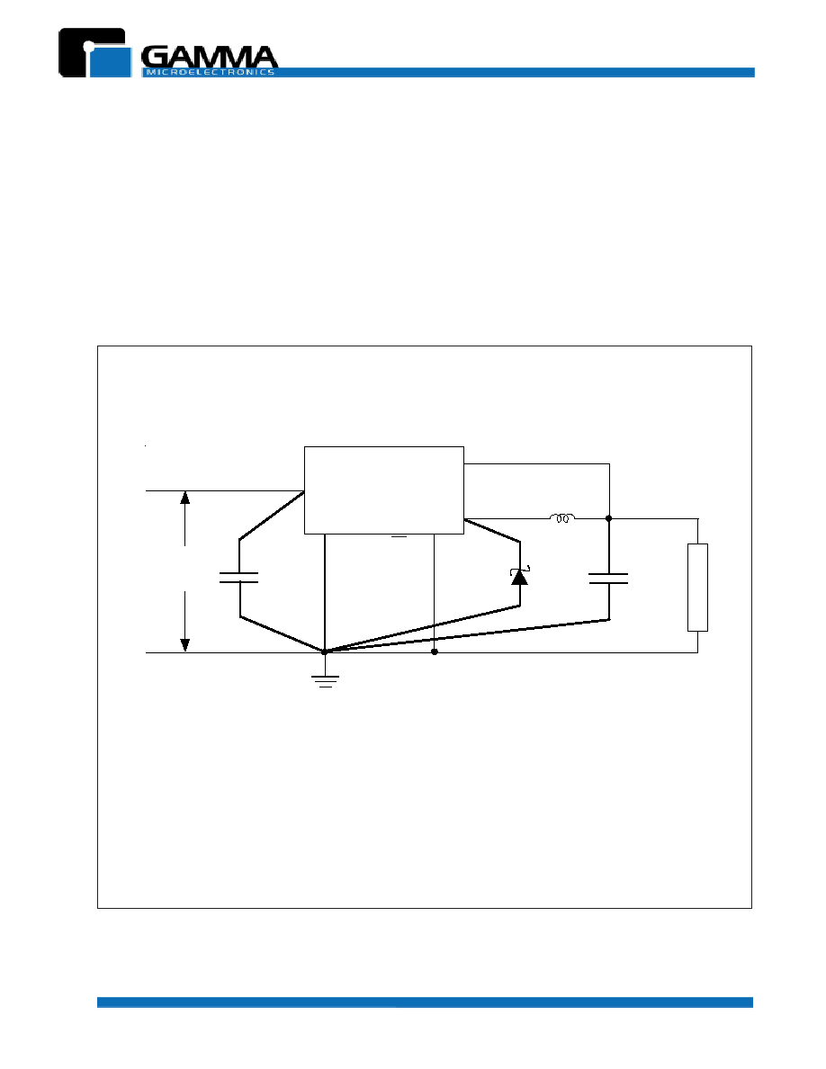
TEST CIRCUIT AND LAYOUT GUIDELINES
Careful layout is important with any switching regulator. Rapidly switching currents associated with wiring
inductance generate voltage transients which can cause problems. To minimize inductance and ground loops,
the lengths of the leads indicated by heavy lines in Figure 2 below should be kept as short as possible. Single-
point grounding (as indicated in Figure 2) or ground plane construction should be used for best results. When
using the Adjustable version, place the programming resistors as close as possible to the GM7230, to keep the
sensitive feedback wiring short.
C
IN
-- 470 µF, 50V, Aluminum Electrolytic
C
OUT
-- 2200 µF, 25V, Aluminum Electrolytic
D1 -- 5A, 40V Schottky
L1 -- 68 µH, Pulse Eng.