 | ÐлекÑÑоннÑй компоненÑ: GF3443 | СкаÑаÑÑ:  PDF PDF  ZIP ZIP |
/home/web/doc/html/ge/212975
Features
· Advanced trench process technology
· High density cell design for ultra low on-resistance
· Popular SOT-23-6L package with copper lead-frame
for superior thermal and electrical capabilities
· Compact and low profile
· 2.5V rated
Maximum Ratings and Thermal Characteristics
(T
A
= 25°C unless otherwise noted)
Parameter
Symbol
Limit
Unit
Drain-Source Voltage
V
DS
20
V
Gate-Source Voltage
V
GS
±
12
Continuous Drain Current
T
A
= 25°C
I
D
4.4
A
T
J
= 150°C
T
A
= 70°C
3.5
A
Pulsed Drain Current
I
DM
20
Maximum Power Dissipation
T
A
= 25°C
P
D
2.0
W
T
A
= 70°C
1.3
Operating Junction and Storage Temperature Range
T
J
, T
stg
55 to 150
°C
Maximum Junction-to-Ambient
(1)
R
JA
62.5
°C/W
Note: (1) Surface Mounted on FR4 Board, t
5 sec.
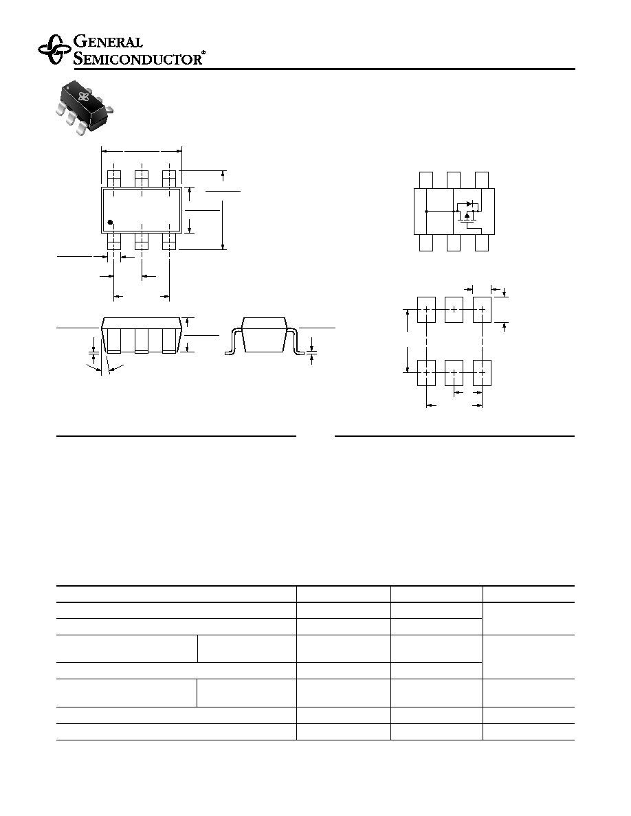
Mechanical Data
Case: SOT-23-6L package
Terminals: Leads solderable per MIL-STD-750,
Method 2026
Marking Code: 43
GF3443
P-Channel Logic Level
Enhancement-Mode MOSFET
V
DS
20V R
DS(ON)
65
m
I
D
4.4A
5/4/01
Mounting Pad Layout
Pin Configuration (Top View)
SOT-23-6L
T
RENCH
G
EN
F
ET
®
New Product
1
6
2
5
3
4
0.037 (0.95)
Ref.
0.074 (1.9)
Ref.
0.094 (2.4)
0.028 (0.7)
0.039
(1.07)
0.122 (3.10)
0.114 (2.90)
0.067 (1.70)
0.059 (1.50)
0.118 (3.00)
0.106 (2.70)
0.020 (0.50)
0.010 (0.25)
0.004 (0.10)
0.0005 (0.013)
0.075 (1.90)
0.008 (0.20)
0.004 (0.10)
10
°
Typical
0.039 (1.00)
0.036 (0.90)
0.037 (0.95)
Top View
Dimensions in inches
and (millimeters)
Electrical Characteristics
(T
J
= 25°C unless otherwise noted)
Parameter
Symbol
Test Condition
Min
Typ
Max
Unit
Static
Drain-Source Breakdown Voltage
BV
DSS
V
GS
= 0V, I
D
= 250
µ
A
20
--
--
V
Gate Threshold Voltage
V
GS(th)
V
DS
= V
GS
, I
D
= 250
µ
A
0.6
--
--
V
Gate-Body Leakage
I
GSS
V
DS
= 0V, V
GS
=
±
12V
--
--
±
100
nA
Zero Gate Voltage Drain Current
I
DSS
V
DS
= 20V
T
J
= 25°C
--
--
1.0
µ
A
V
GS
= 0V
T
J
= 70°C
--
--
5.0
On-State Drain Current
(1)
I
D(on)
V
DS
5V, V
GS
= 4.5V
15
--
--
A
V
GS
= 4.5V, I
D
= 4.4A
--
50
65
Drain-Source On-State Resistance
(1)
R
DS(on)
V
GS
= 2.7V, I
D
= 3.7A
--
65
90
m
V
GS
= 2.5V, I
D
= 3.5A
--
68
100
Forward Transconductance
(1)
g
fs
V
DS
= 10V, I
D
= 4.4A
--
12
--
S
Dynamic
Total Gate Charge
Q
g
V
DS
= 10V, V
GS
= 4.5V
--
9.6
15
Gate-Source Charge
Q
gs
I
D
= 4.4A
--
1.4
--
nC
Gate-Drain Charge
Q
gd
--
2.8
--
Turn-On Delay Time
t
d(on)
--
10
50
Rise Time
t
r
V
DD
= 10V, R
L
= 10
--
25
60
Turn-Off Delay Time
t
d(off)
I
D
1A, V
GEN
= 4.5V
--
65
100
ns
Fall Time
t
f
R
G
= 6
--
68
80
Input Capacitance
C
iss
V
DS
= 10V, V
GS
= 0V
--
770
--
Output Capacitance
C
oss
f = 1.0MH
Z
--
210
--
pF
Reverse Transfer Capacitance
C
rss
--
140
--
Source-Drain Diode
Maximum Diode Forward Current
I
S
--
--
--
1.7
A
Diode Forward Voltage
V
SD
I
S
= 1.7A, V
GS
= 0V
--
0.75
1.2
V
Note:
(1) Pulse test; pulse width
300
µ
s,
duty cycle
2%
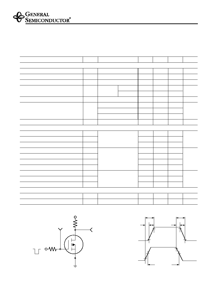
GF3443
P-Channel Logic Level
Enhancement-Mode MOSFET
G
D
S
V
IN
V
DD
V
GEN
R
G
R
D
V
OUT
DUT
Input, V
IN
t
d(on)
Output, V
OUT
t
on
t
r
t
d(off)
t
off
t
f
INVERTED
90%
10%
10%
90 %
50%
50%
10%
90%
PULSE WIDTH
Switching
Test Circuit
Switching
Waveforms
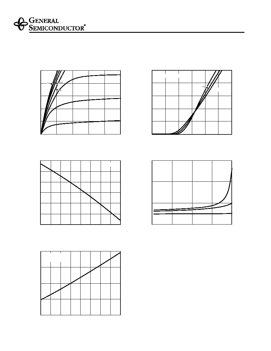
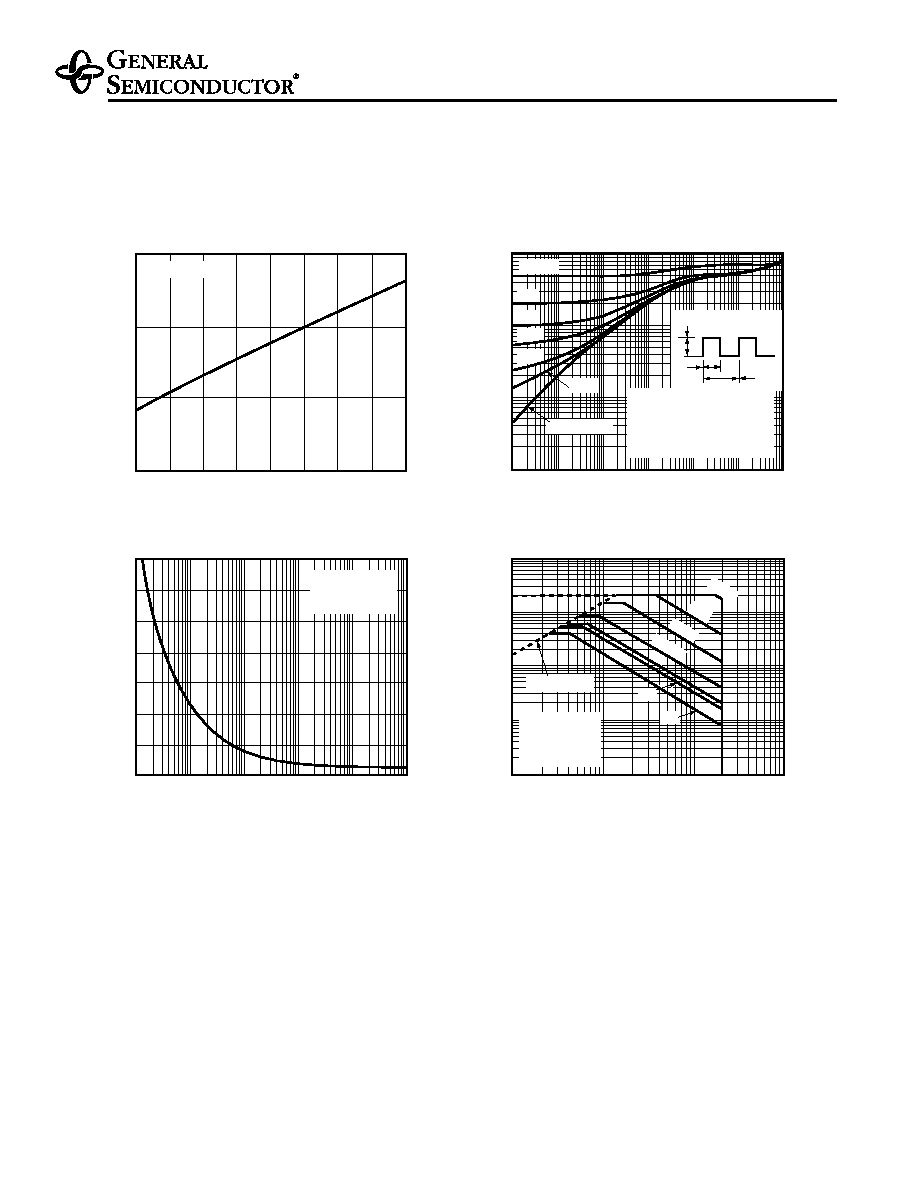
GF3443
P-Channel Logic Level
Enhancement-Mode MOSFET
Ratings and
Characteristic Curves
(T
A
= 25°C unless otherwise noted)
0
4
8
16
20
0
1
2
3
4
5
Fig. 1 Output Characteristics
0
0
5
10
15
20
Fig. 4 On-Resistance
vs. Drain Current
0
4
12
8
16
20
0
0.5
1
1.5
2
3
2.5
Fig. 2 Transfer Characteristics
12
-- 1.5V
0.8
0.6
1.2
1.4
1
Fig. 5 On-Resistance
vs. Junction Temperature
V
GS
= --4.5V
I
D
= --4.4A
--
55
°
C
--2.7V
Fig. 3 Threshold Voltage
vs. Temperature
I
D
= --250
µ
A
--
I
D
-
-
Drain-to-Source Current (A)
R
DS(ON)
-
-
On-Resistance (
)
-- I
D
-- Drain Current (A)
--
I
D
-
-
Drain Current (A)
--V
GS
-- Gate-to-Source Voltage (V)
R
DS(ON)
-
-
On-Resistance (Normalized)
T
J
-- Junction Temperature (
°
C)
--
V
GS(th)
-
-
Gate-to-Source
Threshold V
oltage (V)
T
J
-- Junction Temperature (
°
C)
--
50
--
25
25
50
75
100
125
150
0
--
50
--
25
25
50
75
100
125
150
0
0.5
0.6
0.7
0.8
0.9
1.0
0.4
--V
DS
-- Drain-to-Source Voltage (V)
-- 3.5V
-- 2.5V
-- 4.0V
25
°
C
V
GS
= --4.5V
-- 2.0V
V
GS
=
-- 4.5V
V
DS
= -- 10V
T
J
= 125
°
C
0.1
0.2
0.3
-- 3.0V
--2.5V
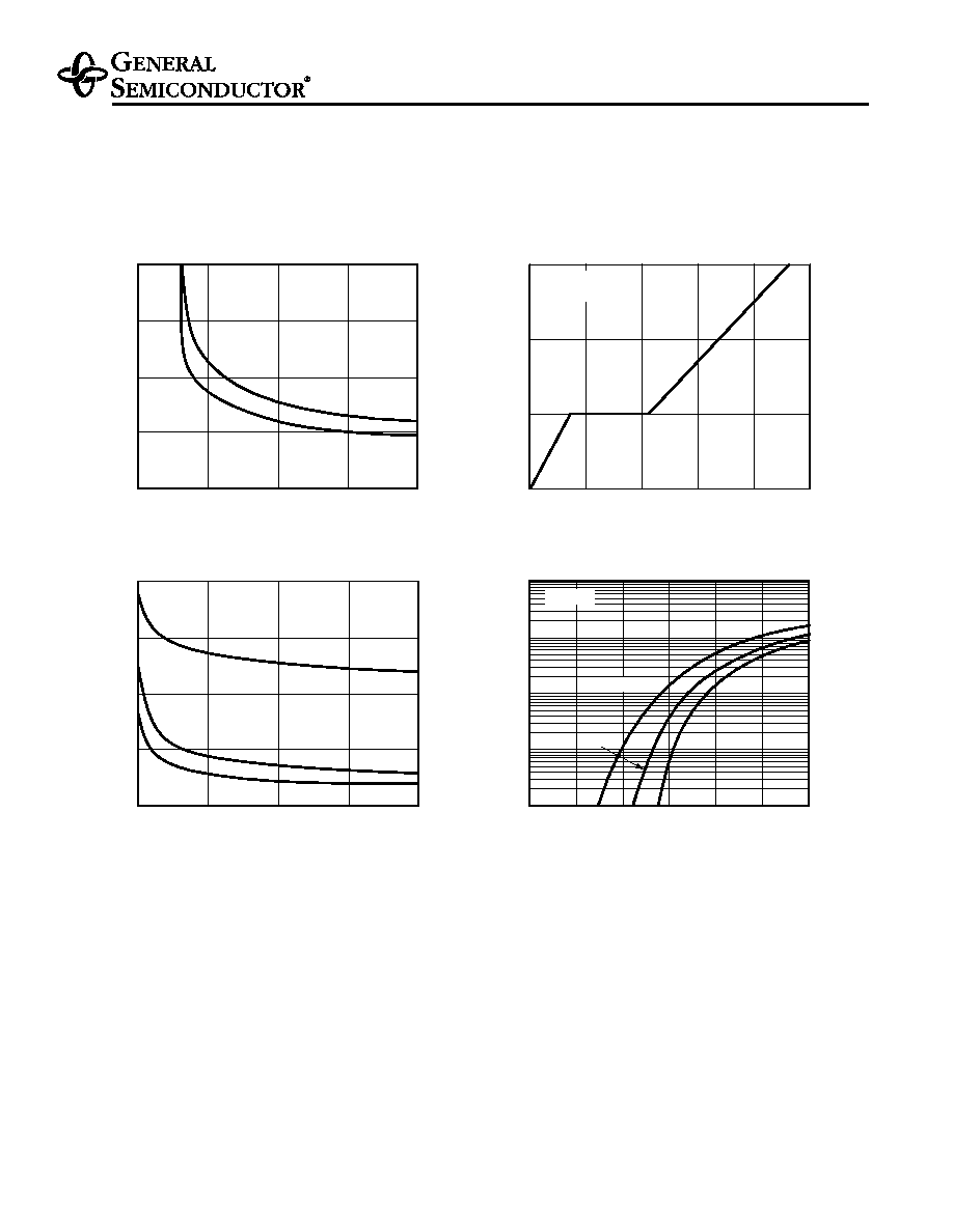
GF3443
P-Channel Logic Level
Enhancement-Mode MOSFET
Ratings and
Characteristic Curves
(T
A
= 25°C unless otherwise noted)
0.01
0.1
1
10
100
0
0.2
0.4
0.6
0.8
1
1.2
T
J
= 125
°
C
Fig. 9 Source-Drain Diode
Forward Voltage
V
GS
= 0V
0
1.5
3
4.5
0
2
4
Fig. 7 Gate Charge
6
8
10
V
DS
= --10V
I
D
= --4.4A
0
300
600
900
1200
0
5
10
15
20
Fig. 8 Capacitance
C
iss
C
rss
f = 1MH
Z
V
GS
= 0V
--
I
S
-
-
Source Current (A)
--V
SD
-- Source-to-Drain Voltage (V)
Q
g
-- Gate Charge (nC)
--
V
GS
-
-
Gate-to-Source V
oltage (V)
C -
-
Capacitance (pF)
--V
DS
-- Drain-to-Source Voltage (V)
--55
°
C
C
oss
25
°
C
0
0.05
0.1
0.15
0.2
1
2
3
4
5
Fig. 6 On-Resistance
vs. Gate-to-Source Voltage
I
D
= --4.4A
R
DS(ON)
-
-
On-Resistance (
)
--V
GS
-- Gate-to-Source Voltage (V)
T
J
= 125
°
C
25
°
C
GF3443
P-Channel Logic Level
Enhancement-Mode MOSFET
Ratings and
Characteristic Curves
(T
A
= 25°C unless otherwise noted)
Fig. 13 Maximum Safe Operating Area
0.0001 0.001
0.01
0.01
0.001
0.1
0.1
1
1
10
100
--
I
D
--
Drain Current (A)
--V
DS
--
Drain-Source Voltage (V)
R
JA
(norm)
--
Normalized Thermal
Impedance
Pulse Duration (sec.)
Single Pulse
0.01
0.001
0.1
0
0.01
0.1
0.1
1
1
10
100
10
100
10
20
30
40
50
60
70
1
10
100
Fig. 12 Power vs. Pulse Duration
Power (W)
Pulse Duration (sec.)
Single Pulse
R
JA
= 78
°
C/W
T
A
= 25
°
C
V
GS
= --4.5V
Single Pulse
R
JA
= 78
°
C/W
T
A
= 25
°
C
R
DS(ON)
Limit
100
µ
s
1ms
10ms
100ms
1s
DC
10s
D = 0.5
0.2
0.01
0.1
t
1
t
2
P
DM
1. Duty Cycle, D = t
1
/t
2
2. R
JA
(t) = R
JA(norm)
*R
JA
3. R
JA
= 78
°
C/W
4. T
J
- T
A
= P
DM
* R
JA
(t)
0.05
0.02
Fig. 11 Thermal Impedance
24
25
27
26
Fig. 10 Breakdown Voltage vs.
Junction Temperature
I
D
= --250
µ
A
-
-BV
DSS
-
-
Drain-to-Source
Breakdown V
oltage (V)
T
J
-- Junction Temperature (
°
C)
--50
--25
25
50
75
100
125
0
150