 | ÐлекÑÑоннÑй компоненÑ: GF4412 | СкаÑаÑÑ:  PDF PDF  ZIP ZIP |
/home/web/doc/html/ge/171974
Features
· Advanced Trench Process Technology
· High Density Cell Design for Ultra Low
On-Resistance
· Specially Designed for Low Voltage DC/DC
Converters
· Fast Switching for High Efficiency
Maximum Ratings and Thermal Characteristics
(T
A
= 25°C unless otherwise noted)
Parameter
Symbol
Limit
Unit
Drain-Source Voltage
V
DS
30
V
Gate-Source Voltage
V
GS
±
20
Continuous Drain Current
T
A
= 25°C
I
D
7
T
J
= 150°C
(1)
T
A
= 70°C
5.8
A
Pulsed Drain Current
I
DM
30
Continuous Source Current (Diode Conduction)
(1)
I
S
2.3
Maximum Power Dissipation
(1)
T
A
= 25°C
P
D
2.5
W
T
A
= 70°C
1.6
Operating Junction and Storage Temperature Range
T
J
, T
stg
55 to 150
°C
Maximum Junction-to-Ambient
(1)
Thermal Resistance
R
JA
50
°C/W
Notes: (1) Surface mounted on FR4 board, t
10 sec.
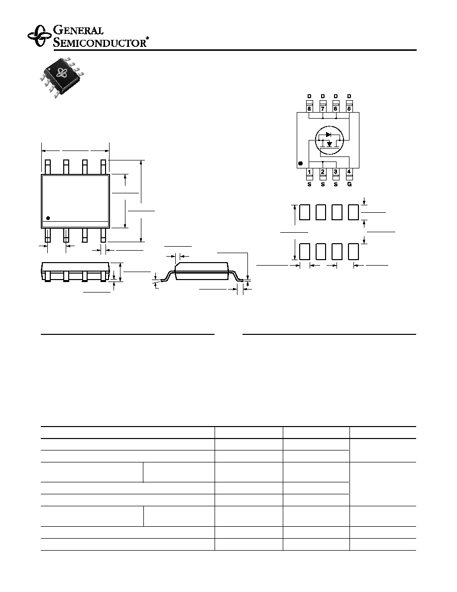
Mechanical Data
Case: SO-8 molded plastic body
Terminals: Leads solderable per MIL-STD-750,
Method 2026
High temperature soldering guaranteed:
250°C/10 seconds at terminals
Mounting Position: Any Weight: 0.5g
GF4412
N-Channel Enhancement-Mode MOSFET
V
DS
30V R
DS(ON)
28
m
I
D
7A
7/10/01
5
1
4
0.244 (6.20)
0.228 (5.79)
8
0.157 (3.99)
0.150 (3.81)
0.020 (0.51)
0.013 (0.33)
0.050 (1.27)
0.009 (0.23)
0.004 (0.10)
0.197 (5.00)
0.189 (4.80)
0.069 (1.75)
0.053 (1.35)
0.019 (0.48)
0.010 (0.25)
x 45
°
0
°
8
°
0.050(1.27)
0.016 (0.41)
0.009 (0.23)
0.007 (0.18)
Dimensions in inches
and (millimeters)
SO-8
T
RENCH
G
EN
F
ET
®
0.245 (6.22)
Min.
0.035 (0.889)
0.025 (0.635)
0.050 typ.
(1.27)
0.165 (4.19)
0.155 (3.94)
0.05 (1.27)
0.04 (1.02)
Mounting Pad Layout
Electrical Characteristics
(T
J
= 25°C unless otherwise noted)
Parameter
Symbol
Test Condition
Min
Typ
Max
Unit
Static
Drain-Source Breakdown Voltage
BV
DSS
V
GS
= 0V, I
D
= 250
µ
A
30
V
Gate Threshold Voltage
V
GS(th)
V
DS
= V
GS
, I
D
= 250
µ
A
1
3
V
Gate-Body Leakage
I
GSS
V
GS
= ±20V, V
DS
= 0V
±
100
nA
Zero Gate Voltage Drain Current
I
DSS
V
DS
= 30V, V
GS
= 0V
1
µ
A
V
DS
= 30V, V
GS
= 0V, T
J
= 55°C
5
On-State Drain Current
(1)
I
D(on)
V
DS
5V, V
GS
= 10V
30
A
Drain-Source On-State Resistance
(1)
R
DS(on)
V
GS
= 10V, I
D
= 7A
20
28
m
V
GS
= 4.5V, I
D
= 3.5A
29
42
Forward Transconductance
(1)
g
fs
V
DS
= 15V, I
D
= 7A
16
S
Dynamic
Total Gate Charge
Q
g
16
23
Gate-Source Charge
Q
gs
V
DS
= 15V, I
D
= 2A
2.2
nC
Gate-Drain Charge
Q
gd
V
GS
= 10V
2.4
Turn-On Delay Time
t
d(on)
6
12
Turn-On Rise Time
t
r
V
DD
= 15V, I
D
= 1A
5
10
Turn-Off Delay Time
t
d(off)
V
GEN
= 10V, R
G
= 6
25
37
ns
Turn-Off Fall Time
t
f
R
L
= 15
7
14
Input Capacitance
C
iss
V
DS
= 15V
810
Output Capacitance
C
oss
V
GS
= 0V
150
pF
Reverse Transfer Capacitance
C
rss
f = 1.0MH
Z
75
Source-Drain Diode
Diode Forward Voltage
(1)
V
SD
I
S
= 2A, V
GS
= 0V
0.75
1.3
V
Notes: (1) Pulse test; pulse width
300
µ
s, duty cycle
2%
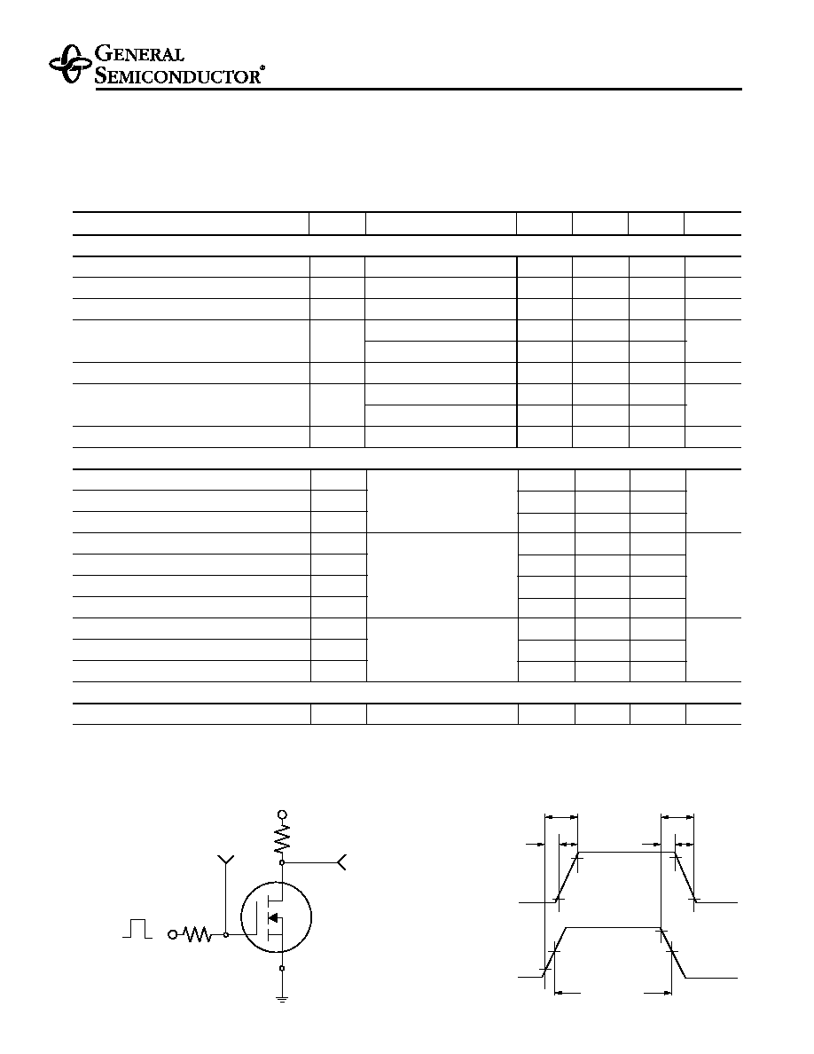
GF4412
N-Channel Enhancement-Mode MOSFET
G
D
S
V
IN
V
DD
V
GEN
R
G
R
D
V
OUT
DUT
Input, V
IN
t
d(on)
Output, V
OUT
t
on
t
r
t
d(off)
t
off
t
f
INVERTED
90%
10%
10%
90 %
50%
50%
10%
90%
PULSE WIDTH
Switching
Test Circuit
Switching
Waveforms
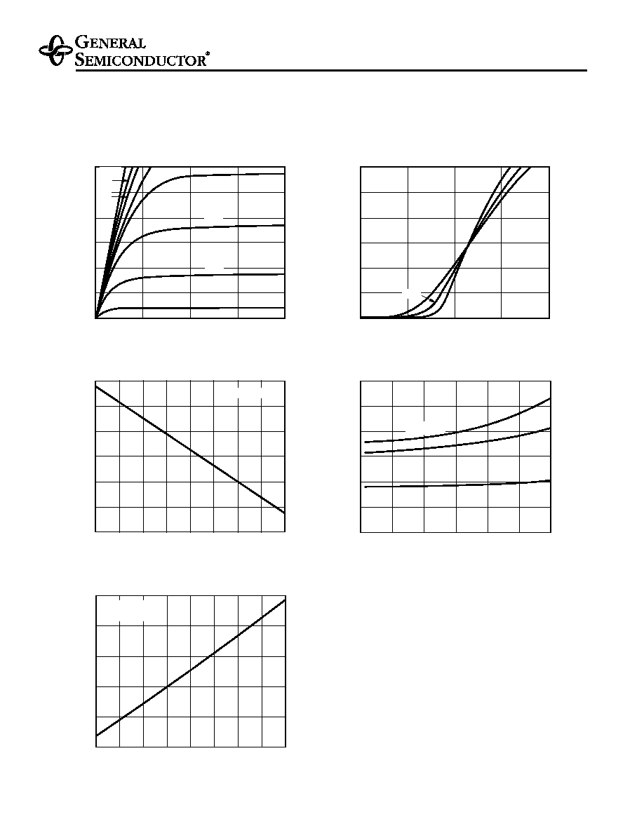
Ratings and
Characteristic Curves
(T
A
= 25°C unless otherwise noted)
0
5
10
15
25
30
0
1
2
3
4
0.02
0.01
0.025
0.015
0.03
0.035
0.04
0
5
10
15
20
25
30
0
10
5
15
25
20
30
1
2
3
4
5
20
2.5V
0.6
1.2
1.4
1.6
0.8
1
V
GS
= 10V
I
D
= 7A
6.0
V
10V
T
J
= 125
°
C
4.0V
4.5V
5.0
V
25
°
C
V
DS
= 10V
V
GS
= 4.5V
5V
0.8
0.6
1
1.2
1.4
1.6
1.8
I
D
= 250
µ
A
3.0V
3.5V
Fig. 1 Output Characteristics
I
D
-
-
Drain Source Current (A)
V
DS
-- Drain-to-Source Voltage (V)
Fig. 4 On-Resistance
vs. Drain Current
R
DS(ON)
-
-
On-Resistance (
)
I
D
-- Drain Current (A)
Fig. 2 Transfer Characteristics
I
D
-
-
Drain Current (A)
V
GS
-- Gate-to-Source Voltage (V)
R
DS(ON)
-
-
On-Resistance
(Normalized)
T
J
-- Junction Temperature (
°
C)
Fig. 5 On-Resistance
vs. Junction Temperature
V
GS(th)
-
-
Threshold V
oltage (V)
T
J
-- Junction Temperature (
°
C)
Fig. 3 Threshold Voltage
vs. Temperature
--55
°
C
--
50
--
25
25
50
75
100
125
150
0
--
50
--
25
25
50
75
100
125
150
0
V
GS
=10V
GF4412
N-Channel Enhancement-Mode MOSFET
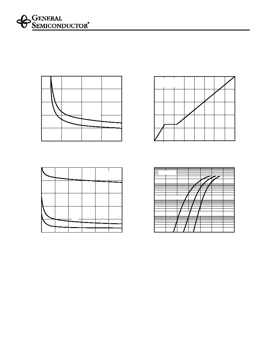
Ratings and
Characteristic Curves
(T
A
= 25°C unless otherwise noted)
0.01
0.1
1
10
100
0
0.2
0.4
0.6
0.8
1
1.2
1.4
T
J
= 125
°
C
--55
°
C
25
°
C
V
GS
= 0V
0
2
4
6
8
10
0
4
6
2
8
10
12
14
16
V
DS
= 15V
I
D
= 7A
0
200
400
600
800
1000
0
5
10
15
30
20
25
C
iss
C
rss
f = 1MHz
V
GS
= 0V
C
oss
I
S
-
-
Source Current (A)
V
SD
-- Source-to-Drain Voltage (V)
Fig. 9 Source-Drain Diode
Forward Voltage
Q
g
-- Gate Charge (nC)
Fig. 7 Gate Charge
V
GS
-
-
Gate-to-Source V
oltage (V)
Fig. 8 Capacitance
C -
-
Capacitance (pF)
V
DS
-- Drain-to-Source Voltage (V)
0
0.02
0.04
0.06
0.08
0.1
2
4
6
8
10
I
D
= 7A
T
J
= 125
°
C
25
°
C
Fig. 6 On-Resistance
vs. Gate-to-Source Voltage
R
DS(ON)
-
-
On-Resistance (
)
V
GS
-- Gate-to-Source Voltage (V)
GF4412
N-Channel Enhancement-Mode MOSFET
Ratings and
Characteristic Curves
(T
A
= 25°C unless otherwise noted)
GF4412
N-Channel Enhancement-Mode MOSFET
36
37
39
40
41
42
38
I
D
= 250
µ
A
Fig. 10 Breakdown Voltage
vs. Junction Temperature
BV
DSS
-
-
Breakdown V
oltage (V)
T
J
-- Junction Temperature (
°
C)
--50
--25
25
50
75
100
125
0
150
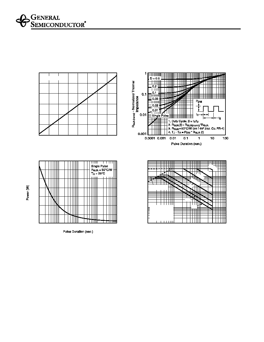
Fig. 11 Transient Thermal
Impedance
Fig. 13 Maximum Safe Operating Area
I
D
-
-
Drain Current (A)
V
DS
-- Drain-Source Voltage (V)
0.01
0.1
0.1
1
1
10
100
10
100
Fig. 12 Power vs. Pulse Duration
V
GS
= 10V
Single Pulse
on 1-in
2
2oz Cu.
T
A
= 25
°
C
R
DS(ON)
Limit
100
µ
s
1ms
10ms
100ms
1s
DC
10s
0.1
0.01
0
10
20
30
40
50
60
70
1
10
100