 | –≠–ª–µ–∫—Ç—Ä–æ–Ω–Ω—ã–π –∫–æ–º–ø–æ–Ω–µ–Ω—Ç: GFB50N03 | –°–∫–∞—á–∞—Ç—å:  PDF PDF  ZIP ZIP |
0
20
40
80
0
1
2
3
4
5
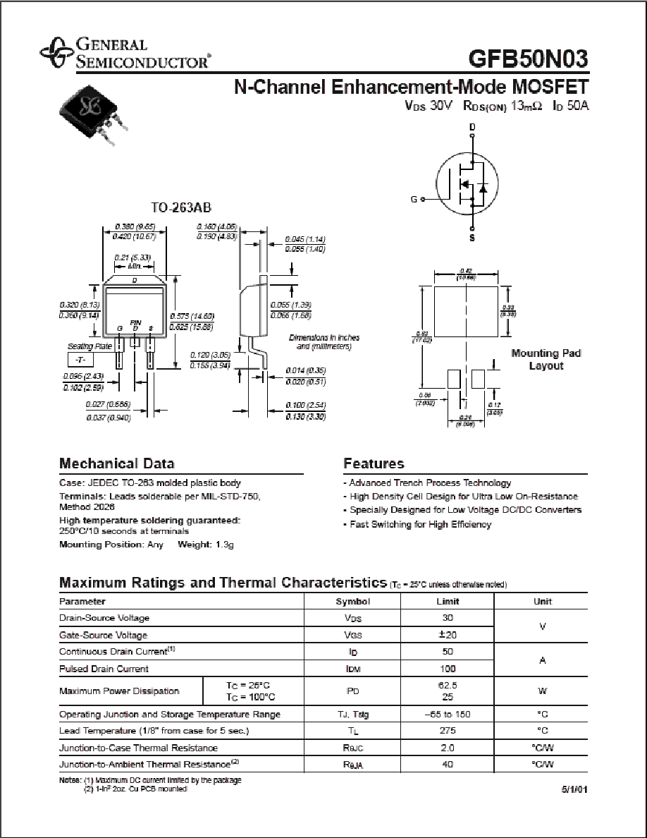
Fig. 1 ≠ Output Characteristics
I
D
-
-
Drain Source Current (A)
V
DS
-- Drain-to-Source Voltage (V)
0
0.01
0.015
0.005
0.02
0.025
0.03
0
20
40
60
80
100
Fig. 4 ≠ On-Resistance
vs. Drain Current
R
DS(ON)
-
-
On-Resistance (
)
I
D
-- Drain Current (A)
0
10
20
40
30
50
60
1
2
3
4
5
Fig. 2 ≠ Transfer Characteristics
I
D
-
-
Drain Current (A)
60
2.5V
0.6
1.2
1.4
1.6
0.8
1
--50
--25
25
50
75
100
125
150
0
R
DS(ON)
-
-
On-Resistance
(Normalized)
T
J
-- Junction Temperature (
∞
C)
Fig. 5 ≠ On-Resistance
vs. Junction Temperature
V
GS
= 10V
I
D
= 25A
6.0V
10V
T
J
= 125
∞
C
--55
∞
C
3.0V
4.0V
4.5V
3.5V
5.0V
25
∞
C
V
DS
= 10V
V
GS
= 4.5V
V
GS
-- Gate-to-Source Voltage (V)
0.8
0.6
1
1.2
1.4
1.6
1.8
--50
--25
25
50
75
100
125
150
0
V
GS(th)
-
-
Threshold V
oltage (V)
T
J
-- Junction Temperature (
∞
C)
Fig. 3 ≠ Threshold Voltage
vs. Temperature
I
D
= 250
µ
A
5V
V
GS
=10V
Ratings and
Characteristic Curves
(T
A
= 25∞C unless otherwise noted)
GFB50N03
N-Channel Enhancement-Mode MOSFET
0
500
1000
1500
2000
2500
0
5
10
15
30
20
25
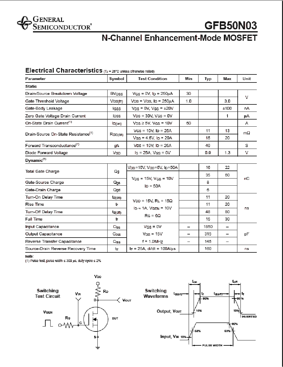
Fig. 8 ≠ Capacitance
C
iss
C
rss
C
oss
f = 1MH
Z
V
GS
= 0V
0
2
4
6
8
10
0
10
20
35
30
Fig. 7 ≠ Gate Charge
V
DS
= 15V
I
D
= 15A
0.01
0.1
1
10
100
0
0.2
0.4
0.6
0.8
1
1.2
T
J
= 125
∞
C
Fig. 9 ≠ Source-Drain Diode
Forward Voltage
25
∞
C
--55
∞
C
V
GS
= 0V
I
S
-
-
Source Current (A)
V
SD
-- Source-to-Drain Voltage (V)
Q
g
-- Charge (nC)
V
GS
-
-
Gate-to-Source V
oltage (V)
C -
-
Capacitance (pF)
V
DS
-- Drain-to-Source Voltage (V)
0
0.005
0.01
0.02
0.03
0.04
0.015
0.025
0.035
2
4
6
8
10
Fig. 6 ≠ On-Resistance
vs. Gate-to-Source Voltage
R
DS(ON)
-
-
On-Resistance (
)
V
GS
-- Gate-to-Source Voltage (V)
I
D
= 25A
T
J
= 125
∞
C
25
∞
C
Ratings and
Characteristic Curves
(T
A
= 25∞C unless otherwise noted)
GFB50N03
N-Channel Enhancement-Mode MOSFET
Ratings and
Characteristic Curves
(T
A
= 25∞C unless otherwise noted)
GFB50N03
N-Channel Enhancement-Mode MOSFET
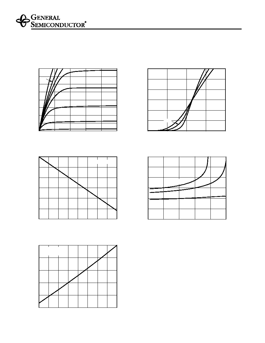
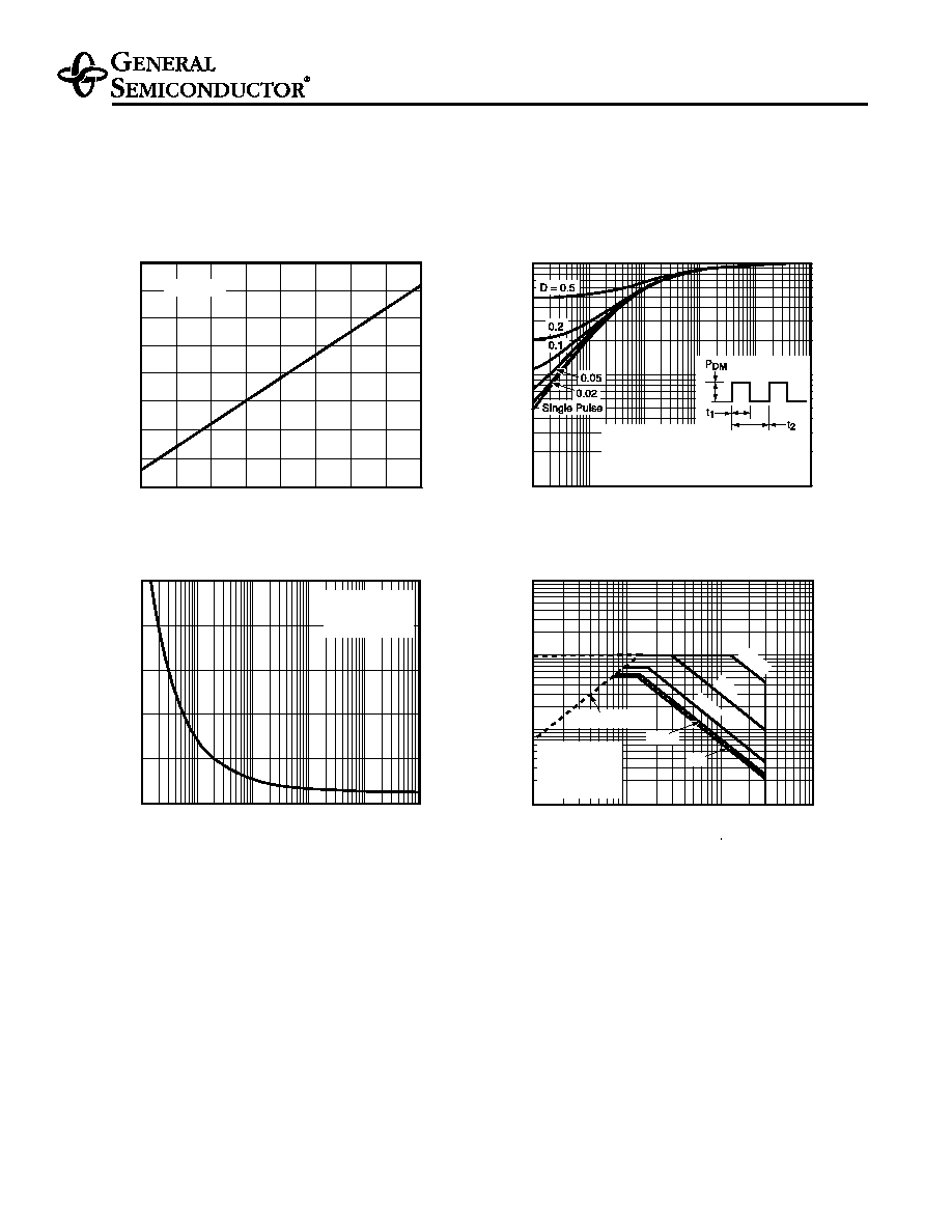
Fig. 11 ≠ Transient Thermal
Impedance
Fig. 13 ≠ Maximum Safe Operating Area
I
D
-
-
Drain Current (A)
V
DS
-- Drain-Source Voltage (V)
0.1
1
1
10
100
1000
0.01
0.1
1
10
100
0.1
0.01
0.001
0.0001
1
10
Fig. 12 ≠ Power vs. Pulse Duration
V
GS
= 10V
Single Pulse
R
JC
= 2.0
∞
C/W
T
A
= 25
∞
C
R
DS(ON)
Limit
100
µ
s
1ms
10m
s
DC
100ms
0.001
0.01
0.0001
0
200
400
600
800
1000
0.1
1
10
1. Duty Cycle, D = t
1
/ t
2
2. R
JA
(t) = R
JA(norm)
*R
JA
3. R
JA
= 2.0
∞
C/W
4. T
J
-- T
A
= P
DM
* R
JA
(t)
37
36
38
40
43
44
39
--50
--25
25
50
75
100
125
0
Fig. 10 ≠ Breakdown Voltage
vs. Junction Temperature
150
I
D
= 250
µ
A
BV
DSS
-
-
Breakdown V
oltage (V)
T
J
-- Junction Temperature (
∞
C)
41
42
Single Pulse
R
JA
= 2.0
∞
C/W
T
C
= 25
∞
C
Pulse Duration (sec.)
Power (W)
Pulse Duration (sec.)
R
JA
(norm)
-
-
Normalized Thermal
Impedance