 | ÐлекÑÑоннÑй компоненÑ: GS1086CT | СкаÑаÑÑ:  PDF PDF  ZIP ZIP |
GS1086.QXD
GS1086
Vishay Semiconductors
formerly General Semiconductor
Document Number 74801
www.vishay.com
12-Mar-02
1
New Product
1.5A Low Dropout
Positive Adjustable Regulator
Description
The GS1086 is a low dropout three terminal regulator with
1.5A output current capability. The output voltage is
adjustable with the use of a resistor divider. For fixed out-
put voltage versions, the output voltage is internally set at
2.5V, 2.85V, 3.3V or 5V. Dropout is guaranteed at a maxi-
mum of 1.5V at maximum output current. Its low dropout
voltage and fast transient response make it ideal for low
voltage microprocessor applications. Internal current and
thermal limiting provides protection against any overload
condition that would create excessive junction temperatures.
Applications
· Post Regulator for Switching Supply
· Battery Chargers
· Constant-Current Regulators
· PC Add-On Card
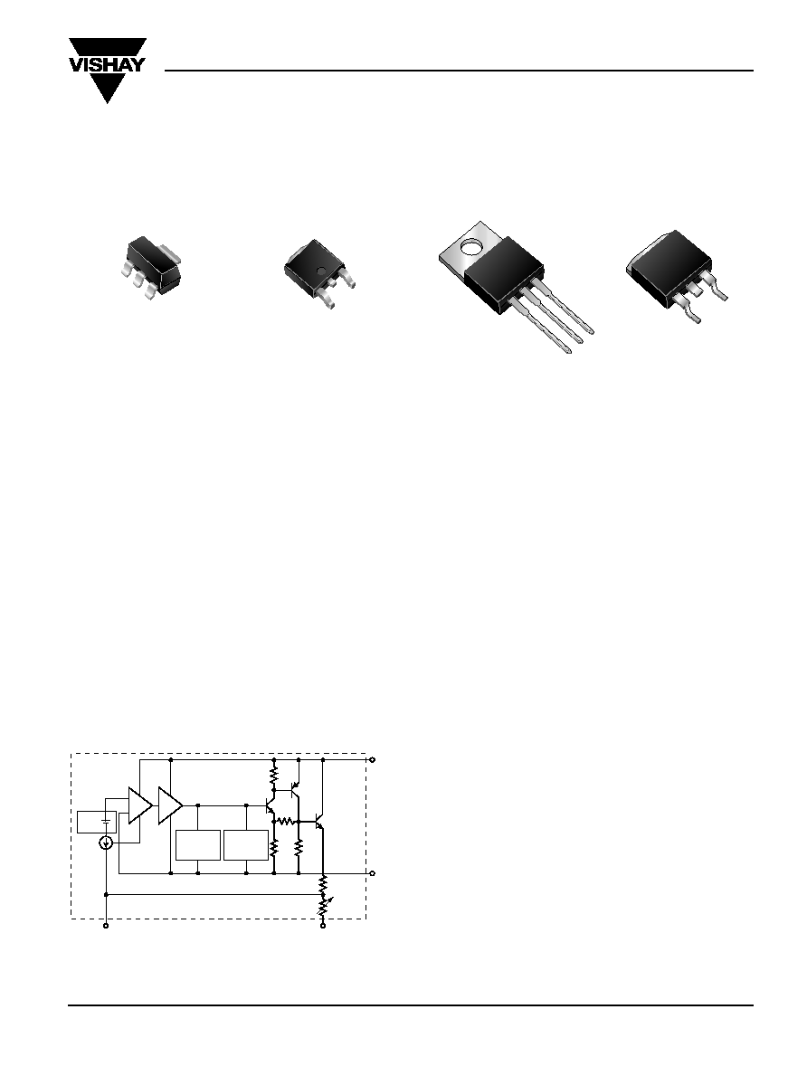
Mechanical Data
Case: TO-220AB, TO-263AB (D
2
PAK),
TO-252 (DPAK) and SOT-223
High temperature soldering guaranteed:
260°C/10 seconds at terminals
Case outlines are on the back page
+
+
--
For
fixed
voltage
device
Thermal
Limit
Current
Amp
Current
Limit
GM
V
OUT
V
IN
ADJ
GND
V
REF
1.25V
55
µ
A
Functional Block Diagram
Features
· Dropout Voltage 1.3V at 1.5A Output Current
· Fast Transient Response
· Line Regulation typically at 0.015%
· Load Regulation typically at 0.1%
· Internal thermal and current limiting
· Adjustable Output Voltage or Fixed 2.5V, 2.85V,
3.3V, 5V
· Standard 3-Pin Power Packages
TO-220AB
TO-263AB
(D
2
Pak)
GS1086CT
GS1086CM
GS1086CE
TO-252
(DPak)
1
2
3
1
2
3
1
2
3
GS1086CST
SOT-223
1
2
3
Pin Definition
1. Adjust/Gnd.
2. V
out (tab)
3. V
in
GS1086
Vishay Semiconductors
formerly General Semiconductor
www.vishay.com
Document Number 74801
2
12-Mar-02
Maximum Ratings and Thermal Characteristics
(T
A
= 25°C unless otherwise noted)
Parameter
Symbol
Value
Unit
Vin Pin to ADJ/GND Pin
Vin
7
V
Thermal Resistance Junction to Case
TO-220AB
3.0
TO-252
R
JC
8.0
°C/W
TO-263AB
3.0
SOT-223
15.0
Operating Junction Temperature Range
T
J
0 to +125
°
C
Storage Temperature Range
T
stg
65 to 150
°C
Electrical Characteristics
(1)
T
J
= 25°C
(2)
, V
IN
= 5V, I
o
= 10mA unless otherwise noted.
Parameter
Symbol
Test Conditions
Min
Typ
Max
Unit
T
J
= 25°C
1.238
1.250
1.262
Reference Voltage
V
REF
0°C
T
J
125°C 1.225
1.250
1.275
V
2.65V
V
IN
7V
10mA
I
o
1.5A
GS1086-2.5
V
IN
= 5V
2.47
2.5
2.53
GS1086-2.85
V
IN
= 5V
2.82
2.85
2.88
GS1086-3.3 V
IN
= 5V
3.26
3.30
3.33
Output Voltage
V
OUT
GS1086-5 V
IN
= 7V
4.95
5.00
5.05
V
GS1086
0.98V
N
V
N
1.02V
N
0°C
T
J
125°C
2.65V
V
IN
7V
10mA
I
o
1.5A
2.65V
V
IN
7V
Line Regulation
REG
line
T
J
= 25°C
0.015
0.2
% V
O
0°C
T
J
125°C
0.02
0.2
10mA
I
o
1.5A
Load Regulation
REG
load
T
J
= 25°C
0.1
0.3
% V
O
0°C
T
J
125°C
0.2
0.4
0°C
T
J
125°C
Dropout Voltage
V
DROP
I
o
= 1.5A
1.3
1.5
V
I
o
= 1.0A
1.25
1.45
I
o
= 500mA
1.2
1.4
Output Current
I
o
0°C
T
J
125°C
1.5
2.0
A
2.65
Vin
7V
Adjust Pin Current
I
adj
10mA
I
o
1.5A 55
120
µ
A
0°C
T
J
125°C
2.65
Vin
7V
Adjust Pin Current Change
I
adj
10mA
I
o
1.5A 0.2
5
µ
A
0°C
T
J
125°C
Temperature Stability
T
S
I
o
= 0.5A
0.8
%V
O
0°C
T
J
125°C
Minimum Load Current
I
LMIN
0°C
T
J
125°C
3
10
mA
Adjustable Version
GS1086
Vishay Semiconductors
formerly General Semiconductor
Document Number 74801
www.vishay.com
12-Mar-02
3
Electrical Characteristics
(1)
(con't.)
T
J
= 25°C
(2)
, V
IN
= 5V, I
o
= 10mA unless otherwise noted.
Parameter
Symbol
Test Conditions
Min
Typ
Max
Unit
Quiescent Current
I
Q
0°C
T
J
125°C
10
14
mA
Fixed Voltage Version
RMS Output Noise
N
10H
Z
f
10 kH
Z
0.003
%V
O
Ripple Rejection Ratio
RR
f = 120 H
Z
, C
O
= 25
µ
F
60
68
dB
C
adj
= 25
µ
F
Thermal Regulation
R
TH
T
A
= 25°C, 30ms Pulse
0.02
0.05
%/W
Long Term Stability
T
A
= 125°C, 1000 Hrs
0.3
%V
O
Notes:
(1) All parameters, except nominal output voltage are specified for the variable voltage version, allowing a wider V
in
Range.
The specified limits also apply for the fixed voltage versions over the allowable input voltage range: GS1086-2.5 (3.9V - 7.0V), GS1086-2.85 (4.25V - 7.0V),
GS1086-3.3 (4.75V - 7.0V), GS1086-5 (6.4V - 7.0V).
(2) To maintain the specified junction temperatures, low duty cycle pulse testing is required for most parameters.
Notes:
V
REF
= V
OUT
V
ADJ
= 1.25V (typ.)
V
OUT
= V
REF
x (1+R2/R1) + I
ADJ
x R2
I
ADJ
= 55
µ
A (typ.)
(1) C1 needed if device is far away from filter capacitors
(2) C2 required for stability
Typical Application Circuit
V
IN
5V
V
OUT
3.3V
C1
10
µ
F
C2
10
µ
F
ADJ
V
REF
1
3
2
R1
125
1%
R2
205
1%
GS1086
Adjustable Voltage Regulator
+
+
V
IN
5V
V
OUT
C1
10
µ
F
C2
10
µ
F
1
3
2
GS1086-2.5
GS1086-2.85
GS1086-3.3
GS1086-5
Fixed Voltage Regulator
+
+
GS1086
Vishay Semiconductors
formerly General Semiconductor
www.vishay.com
Document Number 74801
4
12-Mar-02
Ratings and
Characteristic Curves
(T
A
= 25°C unless otherwise noted)
1.15
1.20
1.25
1.30
1.10
1.05
20
40
60
80
100
120
140
Fig. 2 Dropout Voltage v.s.
Temperature
Dropout V
oltage
(V)
Ambient Temperature (
°
C)
0
20
40
60
80
100
--50
--25
0
25
50
75
100
125
Fig. 4 Adjust Pin Current
Adjust Pin Current (
µ
A)
Temperature (
°
C)
0
--1.6
--1.2
--0.8
--0.4
0.4
0.8
0.0
1.2
1.6
--20
0
20
40
60
80
100
120
140
Fig. 5 Temperature Stability
Output
V
oltage De
viation (%)
Temperature (
°
C)
I
out
= 0.5A
I
OUT
= 1.5A
200
400
800
1000
1200
1400
1600
600
Minim
um Diff
erential
V
oltage (V)
Output Current (mA)
0
0.4
0.8
1.2
1.6
2.0
0
100
1K
100K
10K
1M
Fig. 6 Ripple Rejection
(with Cadj 25
µ
F)
Ripple Rejection (dB)
Frequency (Hz)
20
30
40
50
60
70
80
10
1
2
4
5
6
3
Fig. 3 Minimum Load Current
(Adjustable Version)
Minim
um Oper
ating Current (mA)
Input / Output Differential Voltage (V)
1
2
3
4
5
0
T
J
= 0
°
C
T
J
= 25
°
C
T
J
= 125
°
C
Fig. 1 Dropout Voltage (V
OUT
= 3.3V)
C
OUT
=
25
µ
F
C
OUT
=
25
µ
F
C
OUT
=
10
µ
F
C
OUT
= 10
µ
F
T
J
= 0
°
C
T
J
= 50
°
C
T
J
= 125
°
C
GS1086
Vishay Semiconductors
formerly General Semiconductor
Document Number 74801
www.vishay.com
12-Mar-02
5
--0.1
0.4A
0.1A
--0.05
0
0.05
0.1
40
80
120
160
200
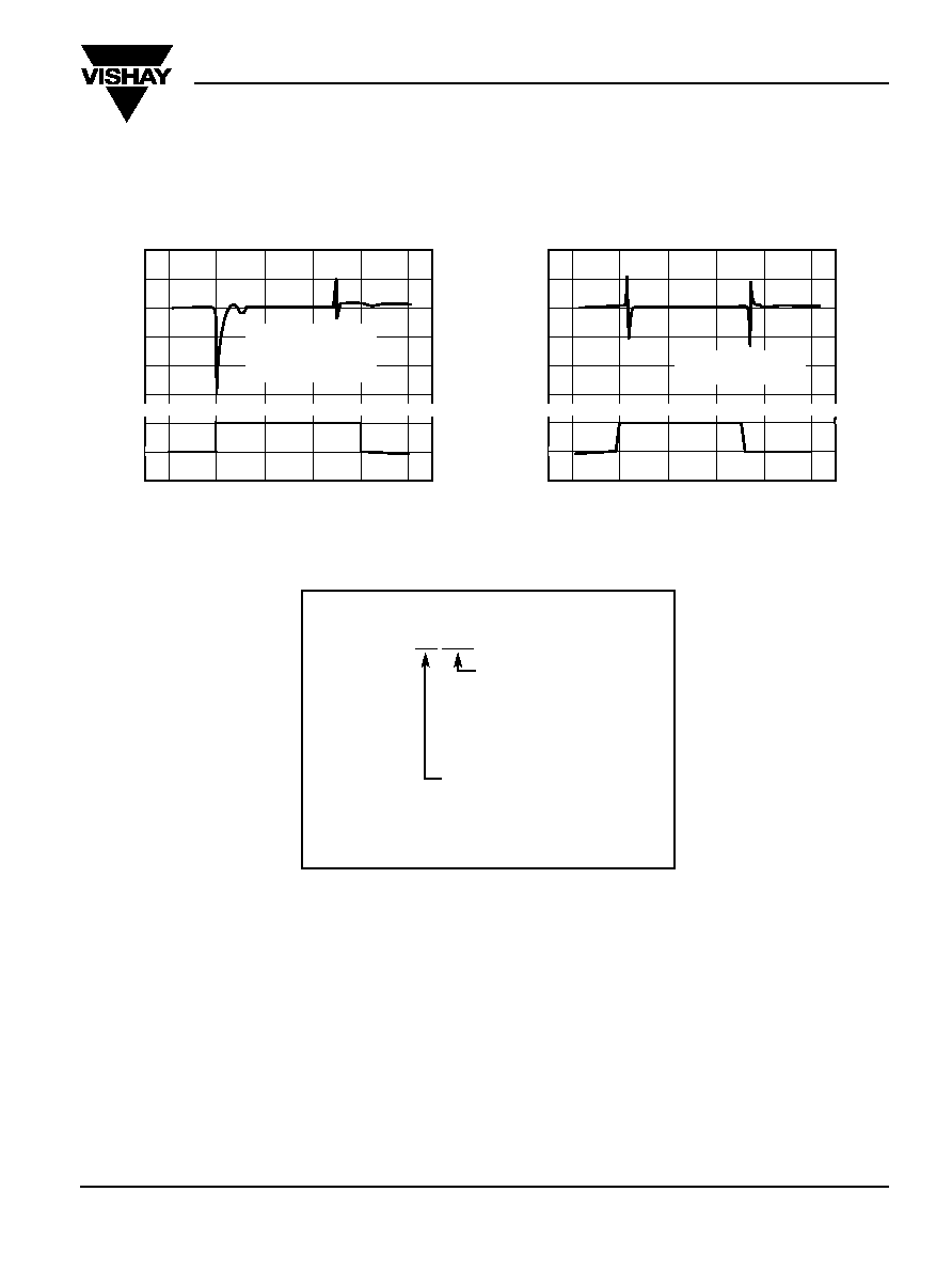
Fig. 7 Load Transient Response
Load Current
Output V
oltage
(V
, AC)
Time (
µ
s)
0
V
IN
=
5V
C
IN
= 1
µ
F
C
OUT
= 10
µ
F (Tantalum)
V
OUT
= 3.3V
--100
7.0
6.0
--50
0
50
10
20
30
40
50
Fig. 8 Line Transient Response
Input V
oltage (V)
Output V
oltage
(mV
, AC)
Time (
µ
s)
0
C
OUT
= 10
µ
F (Tantalum)
V
OUT
= 3.3V
GS1086Cxx xxx
Package Type
ST: SOT-223
T: TO-220
M: TO-263
E: TO-252
Output Voltage
Default: Adj.
2.5: 2.5V
2.85: 2.85V
3.3: 3.3V
5: 5.0V
Ordering Information
Ratings and
Characteristic Curves
(T
A
= 25°C unless otherwise noted)