GSD2004SW
Vishay Semiconductors
formerly General Semiconductor
Document Number 88201
www.vishay.com
14-May-02
1
New Product
High-Voltage Small-Signal Switching Diode
Maximum Ratings and Thermal Characteristics
T
A
= 25∞C unless otherwise noted
Parameter
Symbol
Value
Unit
Continuous Reverse Voltage
V
R
240
V
Peak Repetitive Reverse Voltage
V
RRM
300
V
Peak Repetitive Reverse Current
I
RRM
200
mA
Forward Current (continuous)
I
F
225
mA
Peak Repetitive Forward Current
I
FRM
625
mA
Non-Repetitive Peak Forward Current at tp = 1
µ
s
I
FSM
4.0
A
at tp = 1s
1.0
Power Dissipation
P
tot
350
(1)
mW
Typical Thermal Resistance Junction to Ambiant Air
R
JA
357
(1)
∞C/W
Junction Temperature
T
j
150
∞C
Storage Temperature Range
T
S
≠65 to +150
∞C
Note:
(1) Device on Fiberglass Substrate, see layout on second page
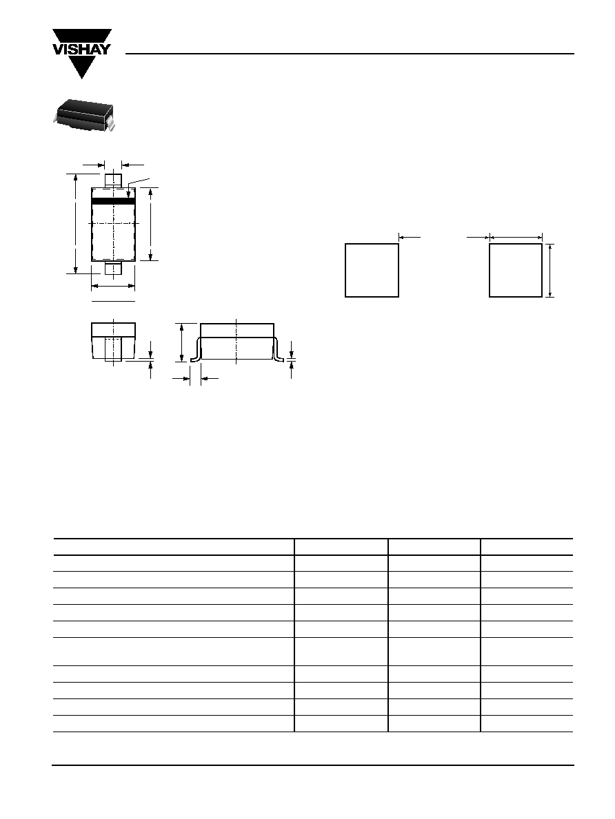
.022 (0.55)
.
112 (2.
85)
.
152 (3.
85)
.067 (1.70)
.
053 (1.
35)
ma
x
.
.010 (0.25)
min.
Cathode Band
.
006 (0.
15)
ma
x
.
Top View
.
140 (3.
55)
.
100 (2.
55)
.055 (1.40)
.004 (0.1)
max.
Features
∑ Silicon Epitaxial Planar Diode
∑ Fast switching diode,especially suited for
applications requiring high voltage capability
SOD-123
Mechanical Data
Case: SOD-123 Plastic Package
Weight: approx. 0.01g
Marking Code: B6
Packaging Codes/Options:
D3/10K per 13" reel (8mm tape), 30K/box
D4/3K per 7" reel (8mm tape), 30K/box
Dimensions in inches
and (millimeters)
Mounting Pad Layout
0.094 (2.40)
0.055 (1.40)
0.055 (1.
40)
GSD2004SW
Vishay Semiconductors
formerly General Semiconductor
www.vishay.com
Document Number 88201
2
14-May-02
Electrical Characteristics
T
J
= 25∞C unless otherwise noted
Parameter
Symbol
Test Condition
Min
Typ
Max
Unit
Reverse Breakdown Voltage
V
BR
I
R
= 100
µ
A
300
--
--
V
Leakage Current
I
R
V
R
= 240V
--
--
100
nA
V
R
= 240V, T
j
= 150∞C
--
--
100
µ
A
Forward Voltage
V
F
I
F
= 20mA
--
0.83
0.87
V
I
F
= 100mA
--
--
1.00
Capacitance
C
tot
V
F
= V
R
= 0
--
--
5.0
pF
f = 1MHz
Reverse Recovery Time
t
rr
I
F
= I
A
= 30mA
--
--
50
ns
I
rr
= 3.0mA, R
L
= 100
Note:
(1 )Device on fiberglass substrate, see layout