P4KE530 AND P4KE550
T
RANS
Z
ORB
TM TRANSIENT VOLTAGE SUPPRESSOR
Steady State Power - 1Watt Reverse Voltage - 530, 550 Volts
FEATURES
Æ Plastic package has Underwriters Laboratory
Flammability Classification 94V-0
Æ Protects TOPSwitch
Æ
Æ Glass Passivated Junction
Æ High temperature soldering guaranteed:
250∞C/10 seconds at terminals
Æ Exellent Clamping capability
Æ Available in unidirectional only
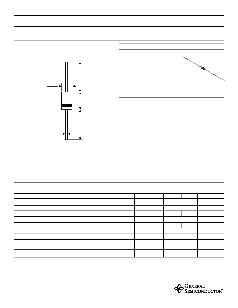
MECHANICAL DATA
Case: JEDEC DO-204AL molded plastic body over
passivated junction
Terminals: Axial leads, solderable per MIL-STD-750,
Method 2026
Polarity: The color band denotes the cathode, which is
positive with respect to the anode under normal TVS
operation
Mounting Position: Any
Weight: 0.012 ounce, 0.3 gram
MAXIMUM RATINGS AND ELECTRICAL CHARACTERISTICS
Ratings at 25∞C ambient temperature unless otherwise specified.
SYMBOLS
P4KE530
P4KE550
UNITS
Steady state power dissipation
(NOTE 3)
P
M(AV)
1.0
Watts
Peak pulse power dissipation
(NOTE 1,2, FIG.1)
P
PPM
Minimum 300
Watts
Minimum breakdown voltage at 100mA
V
(BR)
530
550
Volts
Maximum clamping voltage at 300mA, 10/1000 ms
-
waveform
Vc
660
Volts
Stand-off voltage
V
WM
477
495
Volts
Maximum DC reverse leakage current at V
WM
I
D
5.0
mA
Typical temperature coefficient of V
(BR)
650
mV∞C
Typical capacitance
(NOTE 4)
at 0V
C
J
75
pF
at 200V
45
Operating junction and storage temperature range
T
J
, T
STG
-55 to +150
∞C
NOTES:
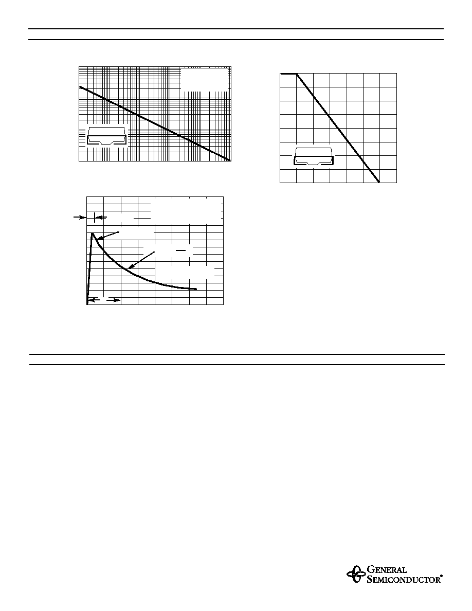
(1) Non-repetitive current pulse, per Fig.3 and derated above 25∞C per - Fig. 2
(2) Peak pulse power waveform is 10/100mS
(3) Lead temperature at 75∞C=T
L
(4) Measured at 1MHz
1/20/99
ADVANCED INFORMATION
0.107 (2.7)
0.080 (2.0)
0.034 (0.86)
0.028 (0.71)
DIA.
1.0 (25.4)
MIN.
1.0 (25.4)
MIN.
0.205 (5.2)
0.160 (4.1)
DIA.
Dimensions are in inches and (millimeters)
Available in uni-directional only
DO-204AL
0
1.0
2.0
3.0
4.0
0
100
150
50
0.1
µ
s
1.0
µ
s
10
µ
s
100
µ
s
1.0ms
10ms
0.1
1.0
10
100
0
50
100
150
0
25
50
75
100
25
75
125
175
1,000
10,000
MAXIMUM RATINGS AND CHARACTERISTIC CURVES P4KE530 AND P4KE550
FIG. 1 - PEAK PULSE POWER RATING CURVE
P
PPM
, PEAK PULSE POWER, kW
td, PULSE WIDTH, sec.
T
A
, AMBIENT TEMPERATURE, ∞C
FIG. 3 - PULSE WAVEFORM
t, TIME, ms
I
PPM,
PEAK PULSE CURRENT
, %
PEAK PULSE POWER (Ppp) or CURRENT
(
IPPM
)
DERA
TING IN PERCENT
AGE, %
NON-REPETITIVE
PULSE WAVEFORM
SHOWN in FIG. 3
T
A
=25∞C
PULSE WIDTH (td) is DEFINED
as the POINT WHERE the PEAK
CURRENT DECAYS
to 50% of I
PPM
tr=10msec.
td
PEAK VALUE
I
PPM
HALF VALUE - I
PPM
2
10/1000msec. WAVEFORM
as DEFINED by R.E.A.
FIG. 2 - PULSE DERATING CURVE
Æ
Respect Thermal Resistance (PCB Layout) - as the temperature coefficient also
contributes to the clamping voltage.
Æ
Select minimum breakdown voltage, so you get acceptable power dissipation and
PCB tie point temperature. Devices with higher breakdown voltage will have a
shorter conduction time and will dissipate less power.
Æ
Clamping voltage is influenced by internal resistance - design approximation is
7V per 100mA slope.
Æ
Keep temperature of TVS lower than TOPSwitch
"
as a recommendation.
Æ
Maximum current is determined by the maximum T
J
and can be higher than
300mA. Contact supplier for different clamping voltage / current arrangements.
Æ
Minimum breakdown voltage can be customized for other applications.
Contact supplier.
APPLICATION NOTES