RGL34A THRU RGL34J
SURFACE MOUNT GLASS PASSIVATED JUNCTION FAST SWITCHING RECTIFIER
Reverse Voltage - 50 to 600 Volts Forward Current - 0.5 Ampere
FEATURES
Plastic package has Underwriters Laboratory
Flammability Classification 94V-0
For surface mount applications
High temperature metallurgically bonded construction
Glass passivated cavity-free junction
Capable of meeting environmental standards of
MIL-S-19500
Fast switching for high efficiency
High temperature soldering guaranteed:
450∞C/5 seconds at terminals. Complete device
submersible temperature of 260∞C for 10 seconds in
solder bath
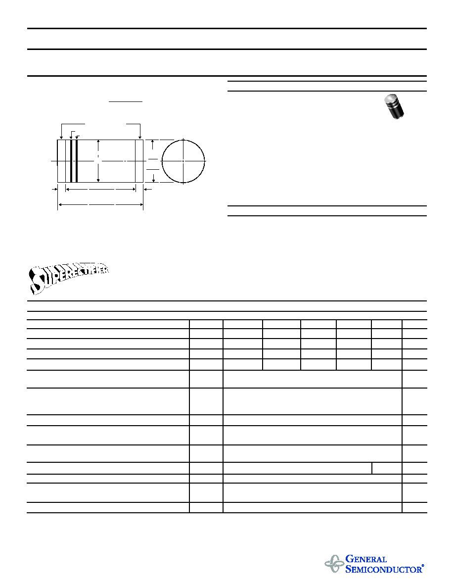
MECHANICAL DATA
Case: JEDEC DO-213AA molded plastic over glass body
Terminals: Plated terminals, solderable per MIL-STD-750,
Method 2026
Polarity: Two bands indicate cathode end - 1st band
denotes device type and 2nd band denotes repetitive peak
reverse voltage rating
Mounting Position: Any
Weight: 0.0014 ounce, 0.036 gram
MAXIMUM RATINGS AND ELECTRICAL CHARACTERISTICS
Ratings at 25∞∞C ambient temperature unless otherwise specified.
Fast switching device: 1st band is Red
SYMBOLS RGL34A
RGL34B
RGL34D
RGL34G
RGL34J
UNITS
Polarity color bands (2nd Band)
Gray
Red
Orange
Yellow
Green
Maximum repetitive peak reverse voltage
V
RRM
50
100
200
400
600
Volts
Maximum RMS voltage
V
RMS
35
70
140
280
420
Volts
Maximum DC blocking voltage
V
DC
50
100
200
400
600
Volts
Maximum average forward rectified current
at T
T
=55∞C
I
(AV)
0.5
Amp
Peak forward surge current
8.3ms single half sine-wave superimposed
on rated load (JEDEC Method)
I
FSM
10.0
Amps
Maximum instantaneous forward voltage at 0.5A
V
F
1.3
Volts
Maximum DC reverse current
T
A
=25∞C 5.0
at rated DC blocking voltage
T
A
=125∞C
I
R
50.0
µ
A
Maximum full load reverse current, full cycle
average T
A
=55∞C
I
R(AV)
30.0
µ
A
Maximum reverse recovery time
(NOTE 1)
t
rr
150
250
ns
Typical junction capacitance
(NOTE 2)
C
J
4.0
pF
Maximum thermal resistance
(NOTE 3)
R
JA
150.0
(
NOTE 4)
R
JT
70.0
∞C/W
Operating junction and storage temperature range
T
J
, T
STG
-65 to +175
∞C
NOTES:
(1) Reverse recovery test conditions I
F
=0.5A, I
R
=1.0A, I
rr
=0.25A
(2) Measured at 1.0 MHz and applied reverse voltage of 4.0 Volts
(3) Thermal resistance from junction to ambient, 0.2 x 0.2" (5.0 x 5.0mm) copper pads to each terminal
(4) Thermal resistance from junction to terminal, 0.2 x 0.2" (5.0 x 5.0mm) copper pads to each terminal
4/98
SOLDERABLE ENDS
1st BAND
2nd BAND
0.022 (0.559)
0.016 (0.406)
0.145 (3.683)
0.131(3.327)
D1=
0.066
0.060
(1.676)
(1.524)
D2 = D1 + 0
- 0.008 (0.20)
1st band denotes type and polarity
2cnd band denotes voltage type
D2
Dimensions in inches and (millimeters)
*
Glass-plastic encapsulation technique is covered by
Patent No.3,996,602 and brazed-lead assembly by Patent No.3,930,306
DO-213AA
P
A
TENTED*
Æ
0
25
50
75
100
125
150
175
0
0.1
0.2
0.3
0.4
0.5
1
10
100
0
2.0
4.0
6.0
8.0
12
0.2
0.4
0.6
0.8
1.0
1
10
1
10
100
1
10
10
1.2
1.4
1.6
0.1
0.01
0
20
40
60
80
100
0.01
0.1
1
10
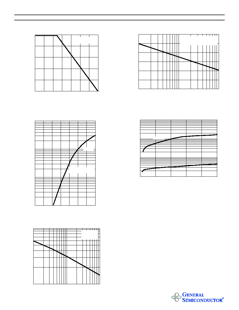
RATINGS AND CHARACTERISTIC CURVES RGL34A THRU RGL34J
FIG. 1 - FORWARD CURRENT
DERATING CURVE
TERMINAL TEMPERATURE, ∞C
A
VERA
GE FOR
W
ARD RECTIFIED
CURRENT
, AMPERES
FIG. 2 - MAXIMUM NON-REPETITIVE PEAK
FORWARD SURGE CURRENT
NUMBER OF CYCLES AT 60 H
Z
PEAK FOR
W
ARD SURGE CURRENT
,
AMPERES
FIG. 3 - TYPICAL INSTANTANEOUS
FORWARD CHARACTERISTICS
FIG. 4 - TYPICAL REVERSE CHARACTERISTICS
INST
ANT
ANEOUS FOR
W
ARD CURRENT
, AMPERES
INST
ANT
ANEOUS REVERSE CURRENT
,
MICR
O
AMPERES
INSTANTANEOUS FORWARD VOLTAGE, VOLTS
FIG. 5 - TYPICAL JUNCTION CAPACITANCE
JUNCTION CAP
A
CIT
ANCE, pF
REVERSE VOLTAGE, VOLTS
T
J
=T
J
max.
8.3ms SINGLE HALF SINE-WAVE
(JEDEC Method)
T
J
= 25∞C
T
J
=25∞C
PULSE WIDTH=300
µ
s
1% DUTY CYCLE
T
J
=25∞C
f=1.0 MHz
Vsig=50mVp-p
RESISTIVE OR
INDUCTIVE LOAD
T
J
=100∞C
PERCENT OF RATED PEAK REVERSE
VOLTAGE, %