ADVANCE INFORMATION
JANUARY 1994
D.S. 3802 1.3
SL5067
MULTI ≠ STANDARD VIDEO MODULATOR
The SL5067 is a video up converter, capable of operating
at frequencies up to 900MHz. It is compatible with both PAL
and NTSC, accepting baseband video and sound inputs and
modulating up to any desired VHF or UHF channel.
Modulated UHF outputs consist of open collectors driving
external 75
W
load resistors for line matching requirements.
Prescaler outputs are also provided enabling the use of a
synthesiser to control oscillator frequency. The SL5067
operates from a 5V supply.
FEATURES
J
5V Operation
J
Symmetrical RF Oscillator Operating to 900MHz
J
Symmetrical RF drive to a frequency synthesiser
J
Video Signal Input Clamp
J
Video Peak White Level Detection and Automatic
Gain Control
J
Control of Video Modulation Index
J
Direct Drive into 75
W
, via Symmetrical open
Collector Outputs
J
ESD Protection
[
J
Picture Carrier to Sound Carrier Ratio Adjustment
J
Low External Component Count
[
ESD Precautions must be observed
APPLICATIONS
J
Video Recorders
J
Cable Systems
J
Video Cameras
J
Personal Computers
J
Video Security Systems
J
In Home Rebroadcast System (LPTV)
16
1
15
2
14
3
13
4
12
5
11
6
10
7
9
8
17
18
19
20
1
18
2
3
4
5
6
7
8
9
16
10
11
12
13
14
15
17
19
20
MOD OUTPUT 2
MOD OUTPUT 1
MOD INDEX
VIDEO INPUT
AGC HOLD
GND
PRESCALER OUTPUT 1
PRESCALER OUTPUT 2
LO INPUT 1
LO OUTPUT 1
GND
V
CC
FM/AM SELECT
AUDIO INPUT
SOUND OSC 1
SOUND OSC 2
GND
LO INPUT 2
LO OUTPUT 2
LO V
CC
GND
V
CC
FM/AM SELECT
AUDIO INPUT
SOUND OSC 1
SOUND OSC 2
GND
LO INPUT 2
LO OUTPUT 2
LO V
CC
MOD OUTPUT 2
MOD OUTPUT 1
MOD INDEX
VIDEO INPUT
AGC HOLD
GND
PRESCALER OUTPUT 1
PRESCALER OUTPUT 2
LO INPUT 1
LO OUTPUT 1
SL5067
SL5067
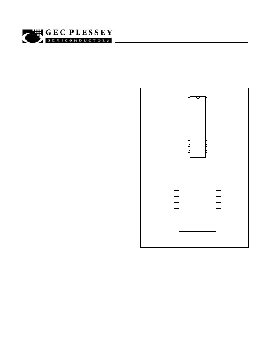
DP20
MP20
Fig. 1 Pin connections ≠ top view
ORDERING INFORMATION
SL5067 /KG/DPAS
SL5067 KG/MPES
SL5067/KG/MPEF (Tape and Reel)

SL5067
2
7
8
PRESCALER OUTPUTS
UHF
OSC
9
10
12
13
TANK
UHF
MIXER
UHF
1
2
MODULATED
OUTPUTS
4
VIDEO
INPUTS
75
W
CLAMP
AGC
VIDEO
MIXER
DRIVER
AUDIO
FM/AM
SELECT
AUDIO
OSC
15
16
TANK
SND
17
AUDIO
INPUT
18
PC/SC ADJUST
3
MOD INDEX
Fig. 2 SL5067 block diagram
ELECTRICAL CHARACTERISTICS
T
amb
= ≠10
∞
C to
)
80
∞
C, V
CC
=
)
4.5V to
)
5.5V. These characteristics are guaranteed over the following conditions
(unless otherwise stated). They apply within the specified ambient temperature and supply voltage ranges.
Characteristics
Pin
Value
Units
Conditions
Characteristics
Pin
Min
Typ
Max
Units
Conditions
Supply Voltage
11, 19
4.5
5.5
V
Supply Current
11, 19
52
mA
V
CC
=5V
LO Prescaler Output Level
7, 8
10
mV RMS
Single ended into 50
W
LO Prescaler Output
Impedance
7, 8
50
W
LO drift with temp from
switch on
10, 12
70
kHz
See note 1
LO variation with supply
10, 12
330
kHz
See note 1, V
CC
= 4.5 to 5.5 V
RF carrier output level
1,2
84
dB
m
V
unmodulated into 50
W
Video Input
4
0.5
1.0
1.5
Vp≠p
Video mod index
1, 2
70
80
%
See note 2
Video Signal/Noise Ratio
1, 2
59
dB
Weighted PAL 200kHz ≠ 5.5MHz
Sound Subcarrier
temperature drift from
switch on
15, 16
4
kHz
See note1
Sound drift with supply
15, 16
2.5
kHz
V
CC
= 4.5 to 5.5V
Audio Input Impedance
17
25
k
W
Audio Input Voltage
reference
17
2
V
Audio Input Level
17
0.88
1
Vp≠p
Measured at pin 17
FM THD
1, 2
1
%
Q = 9,
D
f =
35kHz
AM THD
1.2
1
%
Input level 880mV p≠p
Picture/Sound Carrier Ratio
(FM)
1, 2
10
13
20
dB
R = 0, See note 3
SL5067
3
ELECTRICAL CHARACTERISTICS (cont.)
T
amb
= ≠10
∞
C to
)
80
∞
C, V
CC
=
)
4.5V to
)
5.5V. These characteristics are guaranteed over the following conditions
(unless otherwise stated). They apply within the specified ambient temperature and supply voltage ranges.
Characteristics
Conditions
Units
Value
Pin
Characteristics
Conditions
Units
Max
Typ
Min
Pin
Sound Oscillator FM
Deviation
1, 2
250
kHz/V
C = 120pF, L = 5.6
m
H (Q
L
= 9)
NOTES
1.
Including external components effects
2.
May be increased by use of external resistor, see Fig. 3
3.
May be adjusted by use of external resistor dependent on video content, see Fig. 4
4.
The above measurements assume nominal 80% modulation depth on vision and sound carriers
ABSOLUTE MAXIMUM RATINGS
All voltages are referred to V
EE
=0V
Parameter
Pin
Value
Units
Conditions
Parameter
Pin
Min
Max
Units
Conditions
Supply Voltage
11, 19
≠0.3
7
V
Modulation index
3
≠0.3
V
CC
+0.3
V
Video input
4
≠0.3
V
CC
+0.3
V
Audio input
17
≠0.3
V
CC
+0.3
V
FM/AM select
18
≠0.3
V
CC
+0.3
V
Storage temperature
≠55
+125
∞
C
DP20 thermal resistance,
chip≠to≠ambient
78
∞
C/W
DP20 thermal resistance,
chip≠to≠case
30
∞
C/W
MP20 thermal resistance, chip
to ambient
93
∞
C/W
MP20 thermal resistance,
chip≠to≠case
34
∞
C/W
Power consumption at 5.5V
300
mW
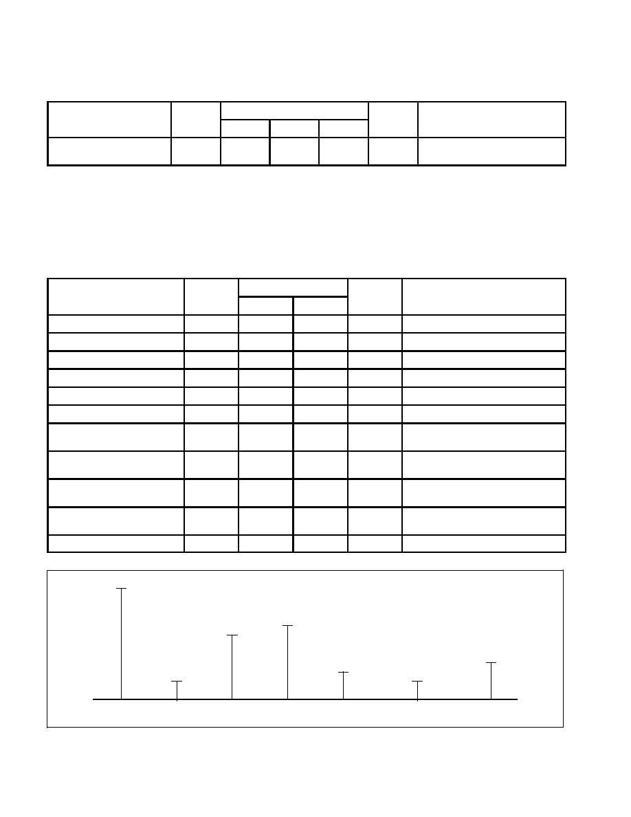
Fig. 3 Frequency spectrum above the Video picture carrier (Q
TANK
= 9)
≠16dB
≠13dB
≠65dB
≠70dB
≠70dB
≠47dB
84dB
m
V
Power levels shown are relative to picture carrier fp typically
fp
fp+(fs≠fc)
1.57MHz
fc
4.43MHz
fs
6MHz
2xfc
8.86MHz
2xfs
12MHz
3xfs
18MHz

SL5067
4
VIDEO
The video signal is applied to pin 4 via a coupling capacitor,
(see Fig.9). This capacitor provides both clamping and black
level hold. The internal peak white AGC can cope with an input
signal of between 0.5 and 1.5 volts peak to peak.The full 9.5
dB AGC range is handled within a 600mV span on this storage
capacitor.
Pin 3 (MOD INDEX) is used to control both RF carrier
amplitude and video polarity, see Fig. 3. Since the video input
is internally AGC'd, varying the carrier amplitude will also
adjust the video modulation index, see Fig. 4.
For example, for a negative modulation (PAL or NTSC) with
an 80% modulation index, pin 3 should be set to 1.1Volts (see
Fig. 4). This voltage corresponds to an unmodulated RF
output level of 82dB
m
V, see Fig. 3.
AUDIO
The sound IF oscillator can operate from 4.5MHz to
6.5MHz to cover all sound standards. The centre frequency is
determined by the Sound IF Tank LC connected between pins
15 and 16.
The centre frequency is given by.
f
0
+
1
2
p
LC
The Q factor of the TANK is given by.
Q
+
1770
2
p
f
0
L
+
1770
2
p
f
0
C
The Q factor of the coil must be high, e.g. >20
Good temperature stability can be achieved by the correct
choice of temperature coefficients for C
sound
and L
sound
.
The Audio signal should be coupled into pin 17 via a 470nF
capacitor. The maximum input level is 1 volts peak to peak.
Selection of AM or FM sound is made via pin 18
(FMAMSEL). The DC value on this pin controls the level of the
sound subcarrier. The crossover point between FM and AM
sound occurs at
Ω
V
CC
(measured at pin 18). Below this
voltage, the modulator is set to FM sound; above it to AM.
Graphs for AM and FM sound subcarrier output levels are
shown in Figs. 6 and 7.
If AM sound is required, it is recommended that a
modulated carrier is fed into the Audio input. Further details of
this are mentioned at the end of the datasheet in the paragraph
marked ``Positive Modulation"
MODULATED RF OUTPUT
The modulated RF outputs from pin 1 and pin 2 consist of
open collectors which should be externally connected to V
CC
via 75
W
resistors. Great care must be taken with the
decoupling of the supply to these outputs.
Both outputs are suitable for driving either 75
W
line, or for
connection to a balun or impedance matching transformer.
This has the added benefit of minimising common mode
coupling, thus giving improved RF performance.
87
85
83
81
79
0.0
1.0
2.0
3.0
4.0
5.0
80dB
m
V
1.4
2.45
VOLTAGE SET ON PIN 3
Fig. 4. Picture carrier, unmodulated RF output level
77

SL5067
5
100
80.0
60.0
40.0
20.0
0.00
0.0
1.0
2.0
3.0
4.0
5.0
80% NEGATIVE
Fig. 5. Modulation index as a function of pin 3 voltage
1.1
2.2
96% POSITIVE
PIN 3 VOLTAGE
MOD
INDEX %
(VIDEO)
NEGATIVE
Fig. 6 FM sound carrier amplitude dB
m
V.
0.0
1.0
2.0
3.0
1.66V
60
55
65
75
RF O/P
LEVEL
dB
m
V
INTO 50
W
ref to ground
PIN18
VOLTAGE
+
≠
PIN 18
45
60
70
40
Fig. 7 AM sound carrier amplitude dB
m
V unmodulated
70
60
50
5V
4.0
3.0
2.0
AUDIO
OUTPUT
LEVEL
dB
m
V
INTO 50
W
PIN18
VOLTAGE
MODULATION
POSITIVE
MODULATION