 | –≠–ª–µ–∫—Ç—Ä–æ–Ω–Ω—ã–π –∫–æ–º–ø–æ–Ω–µ–Ω—Ç: GB3225 | –°–∫–∞—á–∞—Ç—å:  PDF PDF  ZIP ZIP |

Doc.No. 22735 - 3 [Rev. December 2003]
GB3215/GB3225 PRELIMINARY DATA SHEET
1 of 6
G
B
321
5 /
G
B
322
5
FEATURES
∑ highly configurable, versatile DSP platform
∑ high fidelity multi-channel AGC signal processing
∑ 95dB input dynamic range with HRXTM Headroom
Extension
∑ fully programmable via serial data interface
∑ high performance data converters - dual, over-
sampled A/Ds; over-sampled D/A with efficient
switched-mode output power amp
∑ SOUND
DESIGN
TM high-fidelity audio quality
∑ drives zero-bias 2-terminal receivers
∑ multiple communication rates up to 85.3kb/s
∑ thinSTAXTM packaging - CIC size
∑ multi-memory
∑ internal/external volume control
∑ volume control taper determined by external VC
∑ tri-state memory select operation
∑ audible memory change indicator
thinSTAXTM PACKAGING
Hybrid typical dimensions:
0.227 x 0.125 x 0.060 in
(5.76 x 3.18 x 1.52 mm)
DESCRIPTION
The GB3215 (GB3225) hybrid is a programmable DSP
system based on a multi-channel compression circuit. It
can be used as a platform for a wide range of hearing aid
applications. Its extensive programmability and compact
size make it ideal for sophisticated CIC applications. The
reflowable thinSTAXTM packaging enables easy integration
into BTE applications. This very versatile DSP hybrid is
capable of multiple configurations and has a wide range of
functions.
The GB3215 hybrid contains the GC5051 controller chip
and the GA3225 hybrid contains the GC5057 controller
chip. The only difference between the GC5051 and the
GC5057 is in their Power On Reset (POR) behaviour.
For a detailed description of the POR behaviour of the
GC5051 and GC5057 controller chips, please refer to
PARAGONTM DIGITAL Reference Guide
, Document
#20143.
The GB3215 and the GB3225 hybrid code programmed
into the GC5051 and the GC5057 controller chips is "9".
This data sheet is a part of a set of documents available for
this product. Please refer to "
Getting Started with
PARAGONTM DIGITAL
" information note for a list of other
documents.
BLOCK DIAGRAM
PGND
FMIC
FGND
RGND
RREG
FREG
RMIC
T
VC
OUT-
OUT+
MS
SDA
VB
INTERFACE
VC
A/D
FRONTWAVE
CHANNEL 1
CHANNEL 2
CHANNEL 3
CHANNEL 4
EEPROM
REGULATOR
GB3215
A/D
A/D
D/A
HBRIDGE
205n
60n
13n
70n
70n
All resistors in ohms, all capacitors in farads unless otherwise stated.
10
11
6
9
8
7
4
3
12
13
14
1
2
5
S
(GB3225)
PARAGON
TM
DIGITAL
Four Channel
DSP System with F
RONT
W
AVE
Æ
GENNUM CORPORATION
22735 - 3
2 of 6
G
B
321
5 /
G
B
322
5
ABSOLUTE MAXIMUM RATING
PAD CONNECTION
Operating Temperature Range:
-10∞C to 40∞C
Storage Temperature Range:
-20∞C to 70∞C
Absolute Maximum Power Dissipation:
25mW
Maximum Operating Supply Voltage:
1.5VDC
Absolute Maximum Supply Voltage:
2VDC
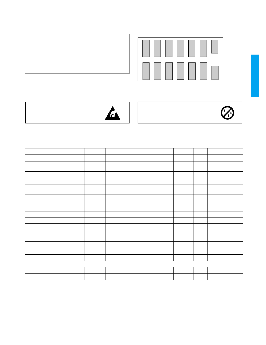
CAUTION
ELECTROSTATIC
SENSITIVE DEVICES
DO NOT OPEN PACKAGES OR HANDLE
EXCEPT AT A STATIC-FREE WORKSTATION
FREG
RREG
RMIC
RGND
VC
SDA
PGND
OUT-
FMIC
FGND
T
MS
VB
OUT+
1
2
3
4
5
6
7
8
9
10
14
13
12
11
CAUTION
LEVEL 3 MOISTURE
SENSITIVE DEVICES
DO NOT OPEN PACKAGES EXCEPT UNDER
CONTROLLED CONDITIONS
ELECTRICAL CHARACTERISTICS
Conditions: Supply Voltage V
B
= 1.3V; Temperature = 25∞C
PARAMETER
SYMBOL
CONDITIONS
MIN
TYP
MAX
UNITS
Hybrid Current
AMP
See current consumption section
-
700
-
µA
Minimum Operating Supply
Voltage
V
BOFF
Ramp down
0.94
1.0
1.05
V
Supply Voltage turn on threshold
V
BON
Ramp up
1.06
1.10
1.16
V
Supply Voltage Hysteresis
90
100
110
mV
Supply Voltage during
Communication
V
BC
During Communication
1.19
1.35
1.5
V
Hybrid Current during
Communication
P
Programming (<5 ms)
-
3.7
-
mA
EEPROM Burn Cycles
Note 2
100k
-
cycles
Low Frequency System Bandwidth
100
140
225
Hz
High Frequency System Bandwidth
15.2
16
16.8
kHz
Total Maximum System Gain
A
V
V
IN
= -95 dBV @ 3kHz; squelch disabled
See Note 1.
81
83
85
dB
Converter Gain
A
CONV
A/D + D/A gain.
27
29
31
dB
Total Harmonic Distortion
THD
V
IN
= -40 dBV
-
0.05
1
%
THD at Maximum Input
THD
M
V
IN
= -15 dBV, HRX - ON
-
1.5
3
%
Clock Frequency
clk
1.945
2.048
2.151
MHz
REGULATOR
Regulator Voltage
V
REG
0.90
0.95
1.00
V
Regulator Supply Rejection
PSRR
REG
-
50
-
dB
GENNUM CORPORATION
22735 - 3
3 of 6
G
B
321
5 /
G
B
322
5
SUPPORT SOFTWARE
All support software for the GB3215 / GB3225 is available from
Gennum Web Site
www.gennum.com/hip/software/index.html
.
INPUT
Input Referred Noise
IRN
Bandwidth 100Hz - 8kHz
-
-108
-106
dBV
Input Impedance
Z
IN
11.2
16
22
k
Anti-alias Filter Rejection
(input referred)
=
clk
-8kHz, V
IN
= -40dBV
-
80
-
dB
Maximum Input Level
-
-15
-
dBV
Input Dynamic Range
HRX - ON, Bandwidth 100Hz - 8kHz
-
95
-
dB
Audio Sample Rate
30.4
32
33.6
kHz
A/D Dynamic Range
Bandwidth 100Hz - 8kHz
-
86
-
dB
OUTPUT
Maximum RMS Output Voltage
0dBFS = 1kHz
-3
-1
1
dBV
D/A Dynamic Range
Bandwidth 100Hz - 8kHz
80
-
-
dB
Output Impedance
Z
OUT
Note 2
-
-
20
VOLUME CONTROL
Volume Control Resistance
R
VC
160
200
240
k
Volume Control Range
A
47.5
48
48.5
dB
MS INPUT
Low State
Lo
0
-
V
REG
/3
V
Open State
Z
V
REG
/3
-
2V
REG
/3
V
High State
Hi
2V
REG
/3
-
V
B
V
SDA INPUT
Logic 0 Voltage
Note 2
0
-
0.3
V
Logic 1 Voltage
Note 2
1
-
1.3
V
SDA OUTPUT
Standby Pull Up Current
1.4
2
2.6
µA
Sync Pull Up Current
450
500
550
µA
Logic 0 Current (Pull Down)
225
250
275
µA
Logic 1 Current (Pull Up)
225
250
275
µA
Synchronization Time
(Synchronization Pulse Width)
T
SYNC
Baud = 0
Baud = 1
Baud = 2
Baud = 3
Baud = 4
Baud = 5
Baud = 6
Baud = 7
237
118
59
29.76
14.88
7.44
3.72
1.86
250
125
62.5
31.25
15.63
7.81
3.91
1.95
263
132
66
32.81
16.41
8.20
4.10
2.05
µs
µs
µs
µs
µs
µs
µs
µs
NOTE 1: Total System Gain consists of: Wideband System Gain + High and Low Independent Channel Gains + Converter Gain
Total System Gain is calibrated during Cal/Config process.
NOTE 2: Sample tested.
ELECTRICAL CHARACTERISTICS
(CONTINUED)
Conditions: Supply Voltage V
B
= 1.3V; Temperature = 25∞C
PARAMETER
SYMBOL
CONDITIONS
MIN
TYP
MAX
UNITS

GENNUM CORPORATION
22735 - 3
4 of 6
G
B
321
5 /
G
B
322
5
Figure 1: Test Circuit
Figure 2: Typical Application Circuit
3k9
3k9
1k
LP FILTER
OUT
VB
INTERFACE
VC
A/D
FRONTWAVE
CHANNEL 1
CHANNEL 2
CHANNEL 3
CHANNEL 4
EEPROM
REGULATOR
GB3215
A/D
A/D
D/A
HBRIDGE
205n
60n
13n
70n
70nF
200k
S
5
10
6
9
8
7
11
4
3
12
13
14
1
2
All resistors in ohms, all capacitors in farads unless otherwise stated.
(GB3225)
VB
VC
MS
200k
GA3214
INTERFACE
VC
A/D
CHANNEL 1
CHANNEL 2
EEPROM
S
REGULATOR
A/D
A/D
D/A
HBRIDGE
205n
60n
13n
70n
2
1
13
12
11
3
4
7
6
8
10
9
5
Knowles or Microtronic
zero-bias receiver
(GA3224)
All resistors in ohms, all capacitors in farads unless otherwise stated.
Knowles or Microtronic microphones
GENNUM CORPORATION
22735 - 3
5 of 6
G
B
321
5 /
G
B
322
5
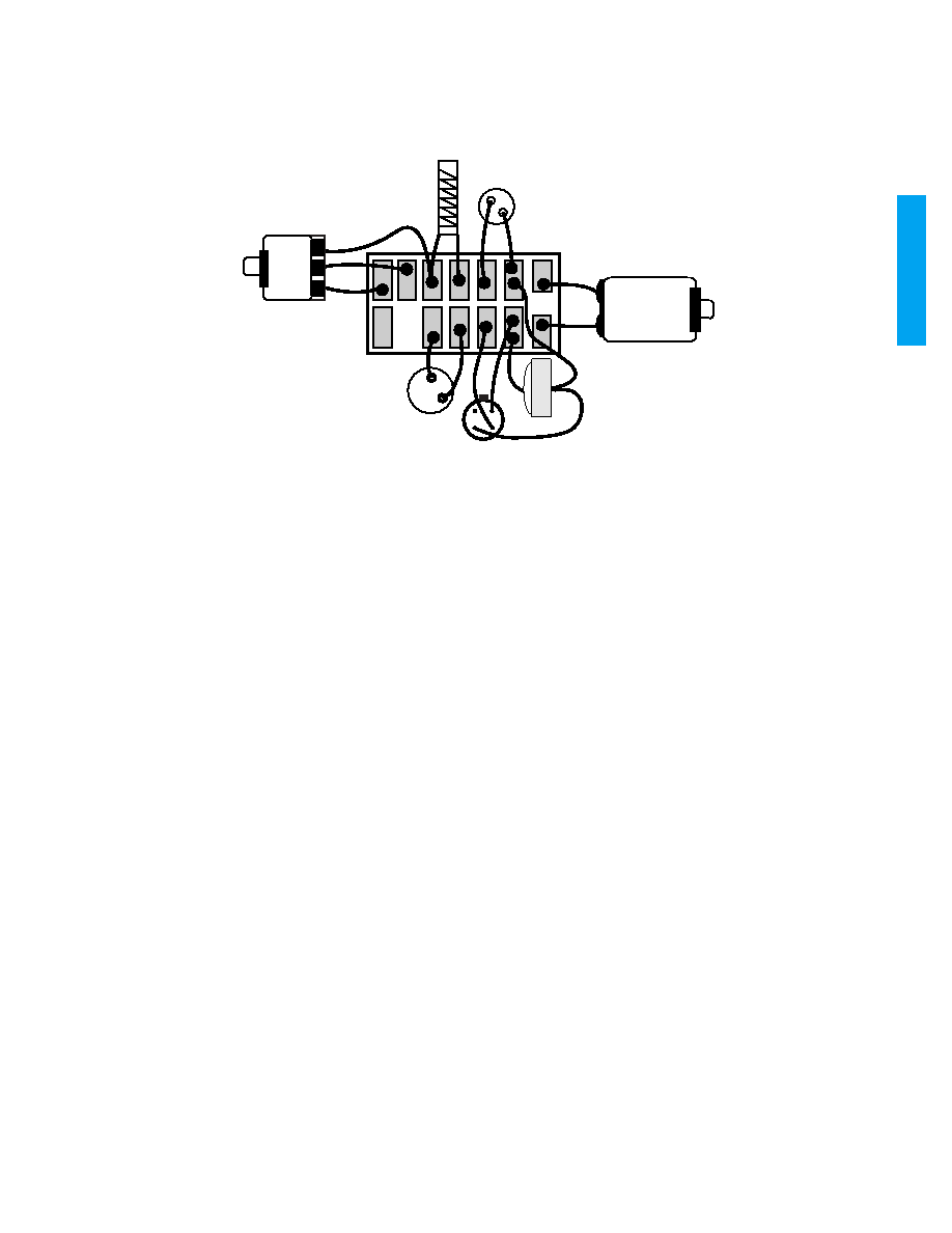
Figure 3: Assembly Diagram
VC
T-coil
SW(N.O.)
+
-
CS44
Mic
+
Zero Biased
Receiver