
GENNUM CORPORATION P.O. Box 489, Stn A, Burlington, Ontario, Canada L7R 3Y3 tel. (905) 632-2996 fax: (905) 632-5946
Japan Branch: A-302, Miyamae Village, 2-10-42 Miyamae, Suginami-ku, Tokyo 168, Japan tel. (03) 3334-7700 fax: (03) 3247-8839
DESCRIPTION
The GB4550 and GB4550A are high performance mono-
lithic video buffer/clamps made on Gennum's LSI process.
They feature a wideband differential amplifier that can be
configured as a gain stage. The output signal voltage is
limited to +2V above the clamp level in order to prevent
damage to crosspoints connected to the output.
The clamping level can be set for normal sync tip clamping
by connecting pin 4 to -0.286 volts. For other applications,
the clamping voltage level can be varied from -5.5 to +5.5
volts.
The GB4550A features a tight delay spread of only
±
0.15
degrees while the GB4550 maintains a
±
1.5 degree delay
spread. Both devices operate from
±
9 to
±
12 V power
supplies and will directly interface with Gennum's video
crosspoint switches.
The 8 pin SIP package is ideally suited for space restricted
board layouts.
APPLICATIONS
∑
Input buffering and clamping to crosspoint switches
∑
Inter - system video signal clamping
FEATURES
∑
adjustable clamp level from -5.5 V to +5.5 V at
±
10 V
supplies.
∑
ultra low differential gain (0.02% typ.) and
differential phase (0.03
∞
typ.)
∑
wideband unity gain: GB4550
±
0.2 dB at 25 MHz
GB4550A
±
0.1 dB at 25 MHz
∑
both drive 150pF loads at full power, flat to 10 MHz.
∑
GB4550A -- tight delay spread of
±
0.15
∞
at colorburst.
∑
convenient 8 pin SIP packaging.
∑
both can be configured as a gain stage with reduced
bandwidth.
Document No. 520 - 34 - 4
GB4550 & GB4550A
Monolithic Video Buffer/Clamp
DATA SHEET
1 2 3 4 5 6 7 8
GB4550 and GB4550A
Pin No.
GB4550
GB4550A
Function
1
+IN
+IN
non-inverting input
2
V
CC
V
CC
positive power supply
3
COMP
NC
frequency compensation or NC
4
V
CL
V
CL
clamp voltage input
5
C
X
C
X
external capacitor
6
V
EE
V
EE
negative power supply
7
-IN
-IN
inverting input
8
OUT
OUT
output
+IN
10pF
C
X
V
CL
COMP
OUT
30k
100k
7mA
Nominal
+
-
-IN
V
CC
V
EE
30k
(+2 V OUTPUT CLAMP)
+
-
(NC on
GB4550A)
SIMPLIFIED CIRCUIT DIAGRAM
ORDERING INFORMATION
Part Number Package Type Temperature Range
GB4550 - CSA 8 pin SIP 0 to 70
o
C
GB4550ACSA 8 pin SIP 0 to 70
o
C
PIN CONNECTIONS
All resistors in ohms, all capacitors in microfarads unless otherwise stated
Revision Date: February 1994

2
520 - 34 - 4
ABSOLUTE MAXIMUM RATINGS
PARAMETER
VALUE
Supply Voltage V
S
±
13.5 V
Operating Temperature Range
0
∞
C
T
A
70
∞
C
Storage Temperature Range
-65
∞
C
T
S
150
∞
C
Lead Temperature (Soldering, 10 Sec)
260
∞
C
Differential Video Input Voltage
±
5 V
Clamp Input Voltage
V
EE
+ 2.5 V
V
CL
V
cc
- 2.5 V
Supply Voltage
V
S
Operating Range
±
9
±
10
±
12
V
+ Supply Current
I+
-
9
13.8
mA
- Supply Current
I-
-
9
13.8
mA
Maximum Input Voltage
Above V
CL
V
IN MAX
2.0
2.25
V
Insertion Loss
I.L.
= 100kHz
-
-
0.03
dB
Full Power Bandwidth
FPBW
-3.0dB, V
IN
= 1V p-p
15
18
-
MHz
Small Signal Bandwidth
SSBW
±
0.2dB, V
IN
= 100mV p-p
20
25
-
MHz
Frequency Response
at 10MHz, V
IN
= 1V p-p
-
0.05
-
dB
Signal Path Delay
¯
D
at 3.58MHz
-
-8
- deg
Delay Tolerance
at 3.58MHz
-
±
1.5
- deg
Full Power Bandwidth
FPBW
-3.0dB, V
IN
= 1V p-p
17
20
-
MHz
Small Signal Bandwidth
SSBW
±
0,1dB, V
IN
=100mV p-p, C
L
=100pF
25
30
-
MHz
Frequency Response
at 10MHz, V
IN
= 1V p-p
-
0.1
-
dB
Signal Path Delay
¯
D
at 3.58 MHz
-
-7.5
- deg
Delay Tolerance
at 3.58MHz
-
±
0.15
- deg
Differential Gain
dg
at 3.58MHz
-
0.02
0.05
%
Differential Phase
dp
at 3.58MHz
-
0.03
0.05
deg
Input Resistance
R
IN
80
100
-
k
Input Capacitance
C
IN
-
2.0
-
pF
Output Resistance
R
OUT
A
V
= +1, = 0 to 10MHz
-
8.6
-
A
V
= +1, = 100MHz
-
53
-
Clamp Voltage Range
V
CL
-5.5
-
+5.5
V
Clamp Accuracy
V
IN
= 1V p-p
-
7
28
mV
PARAMETER
SYMBOL
CONDITIONS
MIN TYP MAX UNITS
ELECTRICAL CHARACTERISTICS
VS =
±
10 V, TA = 0 - 70
∞
C, R
L
= 10k
, CL = 150 pF, CCOMP = 0 pF unless otherwise shown.
POWER
SUPPLIES
SIGNAL
PATH
GB4550
SIGNAL
PATH
GB4550A
SIGNAL
PATH
SIGNAL
PATH
CLAMP
CAUTION
ELECTROSTATIC
SENSITIVE DEVICES
DO NOT OPEN PACKAGES OR HANDLE
EXCEPT AT A STATIC-FREE WORKSTATION
1.8

3
520 - 34 - 4
DETAILED DESCRIPTION
The GB4550(A) is intended for video applications requiring
coarse DC restoration coupled with flat frequency response.
As shown in Figure 1, the signal path features a wide band
operational amplifier designed to be unity gain stable. While
this amplifer is not intended to drive 75
transmission lines,
it is ideal for applications where high capactive loads, up to
several hundred picofarads, must be driven, such as input
buffering and DC restoration of video signals.
Optimal frequency response for the GB4550(A) occurs with
load capacitances in the range of 80 pF to 100 pF as shown in
Figure 4. For smaller loads, an external capacitor can be
added to extend the bandwidth and improve the flatness of the
device response.
The clamping function is achieved through the use of a simple
comparator. The inverting input of the comparator is connected
to the GB4550(A) output, while the non-inverting input is
connected to the clamp voltage reference. For output signal
voltages more positive than the clamp reference the comparator
output is essentially open-circuit, while signal voltages more
negative than the clamp reference result in the charging of C
X
.
The action of the comparator is to provide a positive current
which is fed back to the op-amp non-inverting input under
conditions where the op-amp output is more negative than the
clamp reference voltage. This negative feedback raises the
DC level of the input signal to the point where all signal
fluctuations occur at voltages above the clamp reference
level. This is the desired clamp action.
The input to the op-amp must be AC coupled using an
appropriate size of capacitor, which then acts as a DC "reservoir"
for the corrective level shift.
Under equilibrium conditions the average current supplied by
the comparator output is just sufficient to balance the current
discharging the input capacitor. This discharge current is
simply the input bias current of the op-amp, typically less than
20
µ
A . However, an external resistor can be added to increase
the pull down current. Under dynamic conditions, where the
system is adjusting for a change in the signal level, the
charging current may be in the milliamp range. Because the
corrective current is small under equilibrium conditions, the
error voltage at the comparator input is small also, so clamping
accuracy to within
±
7 mV is achievable.
The clamp circuit makes use of a "peak hold" capacitor, C
X
, at
the output of the comparator . This gives rise to a more
constant voltage at the comparator output which is translated
to a more constant corrective current by an internal 100 k
resistor connected between the comparator output and the
signal input.
To avoid excessive phase shift and consequent instability of
the clamp feedback loop, the peak hold capacitor needs to be
considerably smaller (e.g. 1000 times) than the input coupling
capacitor. If a faster clamp is desirable (e.g. for 60 Hz hum
elimination) the peak hold capacitor can be removed and a
smaller input coupling capacitor employed. In this application
some distortion of the signal "tip" is unavoidable.
+IN
10pF
C
X
V
CL
COMP
OUT
30k
100k
7mA
Nominal
+
-
-IN
V
CC
V
EE
30k
(+2 V OUTPUT CLAMP)
+
-
(NC on
GB4550A)
All resistors in ohms, all capacitors in microfarads unless otherwise stated.
Fig. 1 Simplfied Circuit Diagram
4
520 - 34 - 4
1
5
D.U.T.
4
**C
COMP
**R
COMP
7
SIGNAL IN
FROM
NETWORK
ANALYSER
10n
OUTPUT TO
NETWORK
ANALYSER
2
6
NON-POLAR
0.1
0.1
+10V
-10V
C
LOAD
*22
75
+5V
-5V
5
8
4
0.1
0.1
10k
CLC110
1
0.1
8
3
NOTES
: This circuit can be used for Frequency Response, Delay and Differential Gain and Phase measurements.
* This input capacitor must be shorted out when performing Differential Gain and Phase tests.
** RCOMP
and CCOMP are only used on GB4550.
1
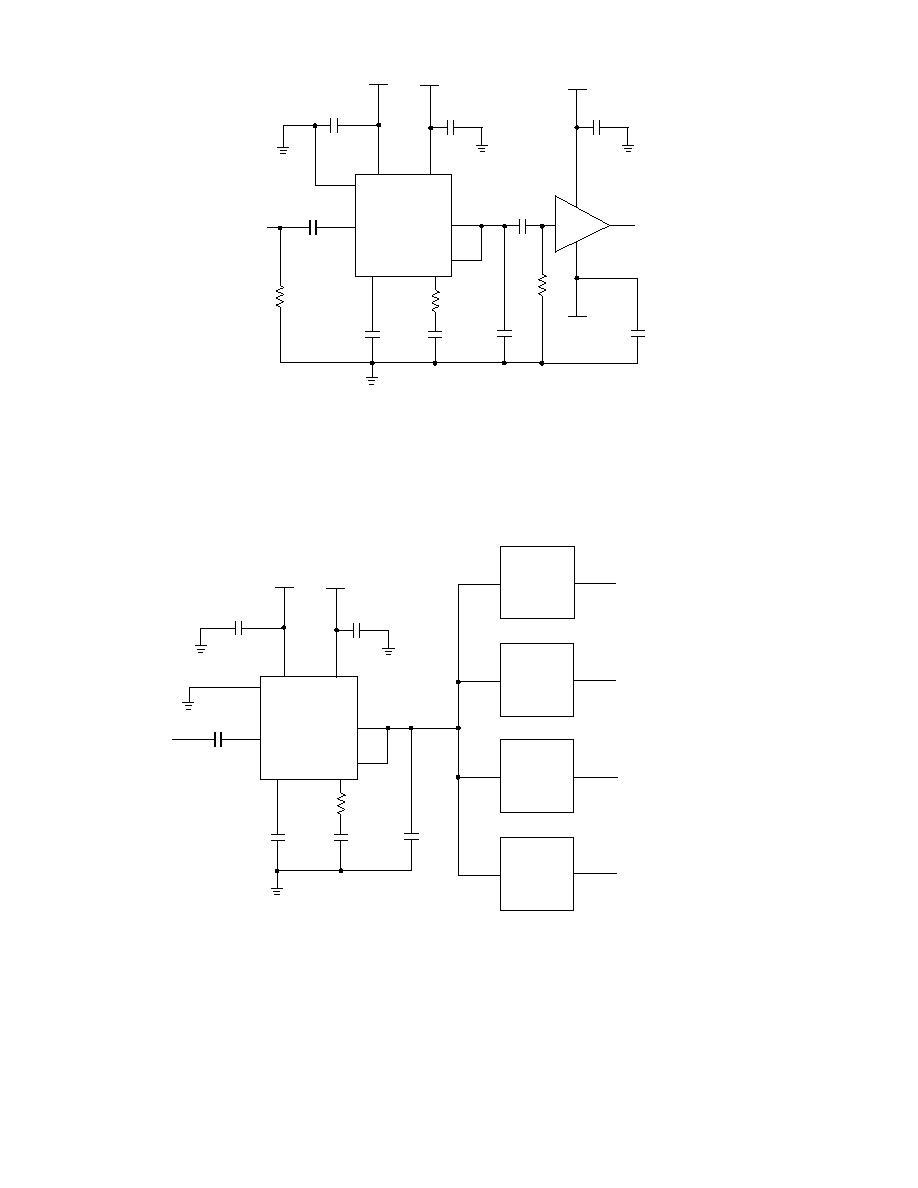
5 3
GB4550
GB4550A
4
GX4314
XPOINT
GX4314
XPOINT
GX4314
XPOINT
GX4314
XPOINT
7
VIDEO
IN
**
10n
VIDEO OUT 1
VIDEO OUT 2
VIDEO OUT 3
VIDEO OUT 4
2
6
NON-POLAR
0.1
0.1
+10V
-10V
C
LOAD
0.1 to 22
*C
COMP
*R
COMP
8
NOTES
: In most applications R
COMP
and C
COMP
will not be needed since the bandwidth depends on the bus capacitance.
In general, the maximum occurs when C
LOAD
is between 82 pF and 100 pF.
They are used to control the roll-off for higher load conditions.
*
Not used on GB4550A.
**
The value of this capacitor should be proportional to the input capacitor used.
The value shown is for a 22
µ
F input capacitor.
All resistors in ohms,
all capacitors in microfarads
unless otherwise stated.
All resistors in ohms,
all capacitors in microfarads
unless otherwise stated.
Fig. 3 Typical Application Circuit
Fig. 2 Test Circuit

5
520 - 34 - 4
DOCUMENT
IDENTIFICATION
PRODUCT PROPOSAL
This data has been compiled for market investigation purposes
only, and does not constitute an offer for sale.
ADVANCE INFORMATION NOTE
This product is in development phase and specifications are
subject to change without notice. Gennum reserves the right to
remove the product at any time. Listing the product does not
constitute an offer for sale.
PRELIMINARY DATA SHEET
The product is in a preproduction phase and specifications are
subject to change without notice.
DATA SHEET
The product is in production. Gennum reserves the right to make
changes at any time to improve reliability, function or design, in
order to provide the best product possible.
Gennum Corporation assumes no responsibility for the use of any circuits described herein and makes no representations that they are free from patent infringement.
© Copyright April 1991 Gennum Corporation. All rights reserved. Printed in Canada.
1
40
0.5
0.4
0.3
0.2
0.1
0
-0.1
-0.2
-0.3
-0.4
-0.5
1
10
40
FREQUENCY (MHz)
GAIN (dB )
150 pF
120 pF
82 pF
C
L
= 180 pF
dp
dg
123456789012345678901234567890121234567890123
123456789012345678901234567890121234567890123
123456789012345678901234567890121234567890123
123456789012345678901234567890121234567890123
123456789012345678901234567890121234567890123
123456789012345678901234567890121234567890123
123456789012345678901234567890121234567890123
123456789012345678901234567890121234567890123
123456789012345678901234567890121234567890123
123456789012345678901234567890121234567890123
123456789012345678901234567890121234567890123
123456789012345678901234567890121234567890123
123456789012345678901234567890121234567890123
123456789012345678901234567890121234567890123
123456789012345678901234567890121234567890123
123456789012345678901234567890121234567890123
123456789012345678901234567890121234567890123
123456789012345678901234567890121234567890123
123456789012345678901234567890121234567890123
123456789012345678901234567890121234567890123
123456789012345678901234567890121234567890123
123456789012345678901234567890121234567890123
123456789012345678901234567890121234567890123
123456789012345678901234567890121234567890123
123456789012345678901234567890121234567890123
123456789012345678901234567890121234567890123
123456789012345678901234567890121234567890123
123456789012345678901234567890121234567890123
123456789012345678901234567890121234567890123
123456789012345678901234567890121234567890123
123456789012345678901234567890121234567890123
123456789012345678901234567890121234567890123
123456789012345678901234567890121234567890123
123456789012345678901234567890121234567890123
123456789012345678901234567890121234567890123
123456789012345678901234567890121234567890123
123456789012345678901234567890121234567890123
-3
-4
-5
-6
-7
-8
-9
-10
Fig. 5 GB4550 Phase Delay Spread
Fig. 4 GB4550 Frequency Response
2
3
4
5
6
FREQUENCY (MHz)
2
6
C
L
= 100 pF
0.5
0.3
0.1
0
-0.1
-0.3
-0.5
1
40
C
L
= 100 pF
C
L
= 82 pF
C
L
= 180 pF
GAIN ( dB )
1
10
40
FREQUENCY (MHz)
-3
-4
-5
-6
-7
-8
-9
-10
2 3 4 5 6
FREQUENCY (MHz)
Fig. 6 GB4550A Frequency Response
Fig. 7 GB4550A Phase Delay Spread
1234
1234
1234
1234
1234
1234
1234
1234
1234
1234
1234
1234
1234
12345
12345
12345
1234
1234
1234
1234
1234
1234
1234
1234
12341234
1234
1234
1234
1234
1234
1234
1234
1234
1234
1234
1234
12345
12345
12345
12345
12345
12345
1234
1234
1234
1234
1234
1234
1234
123
123
123
1234
1234
1234
1234
1234
1234
1234
123
123
123
1234
1234
1234
1234
1234
1234
123
123
123
1234
1234
1234
1234
1234
1234
1234
1234
1234
123
123
123
1234
1234
1234
2
6
C
L
= 100pF
TYPICAL PERFORMANCE CURVES
Unless otherwise shown V
S
=
±
10V
DEGREES
DEGREES
1
10
0.05
0.03
0.01
0
-0.01
-0.03
-0.05
1
3
5
10
FREQUENCY (MHz)
Fig. 8 Differential Gain and Phase
dg
dp
V
IN
= 40 IRE
dg (%) / dp (
∞
)
REVISION NOTE: Detailed Description added