The GB4570 is a high performance video buffer/clamp used
primarily for sync tip clamping of video signals. Key features
include operation from
±
4.5 to
±
13.2 V supply voltages,
±
0.1
dB flatness to 80 MHz and availability of industry standard DIP
and SOIC packages.
In a typical video application, the GB4570 clamps the sync tip
to a known voltage. The clamping level can be set for normal
sync tip clamping by connecting pin 3 to - 0.286 volts. For
applications requiring non-standard sync tip clamping, the
clamping voltage applied to pin 3 may be varied.
The GB4570 features a tight delay spread of only
±
0.15
∞
at
color burst frequencies and less than
±
1 millivolts clamping
distortion.
∑
Sync tip clamping of NTSC, PAL, SECAM and RGB
Video Signals
∑
Input buffering and clamping
∑
Inter-system video signal clamping
DATA SHEET
GENNUM CORPORATION P.O. Box 489, Stn A, Burlington, Ontario, Canada L7R 3Y3 tel. (905) 632-2996 fax: (905) 632-2055
Japan Branch: A-302, Miyamae Village, 2-10-42, Miyamae, Suginami-ku, Tokyo 168, Japan tel. (03) 3247-8838 fax. (03) 3247-8839
GB4570 Monolithic
Video Buffer/Clamp
FEATURES
DESCRIPTION
8 pin PDIP
8 pin SOIC
AVAILABLE PACKAGING
PIN CONNECTIONS
GND
V
IN
V
CLAMP
C
HOLD
V
CC
V
OUT
V
EE
NC
Document No. 521 - 18 - 01
∑
accurate sync tip clamping (
±
2 mV typical)
∑
less than 1 mV clamping distortion
∑
variable clamping voltage (V
EE
+ 3 V to V
CC
-4.5 V)
∑
ultra low differential gain and differential phase
∑
less than
±
0.15
∞
phase delay variation at 3.58 MHz
∑
±
0.1 dB flatness to 80 MHz
∑
±
4.5 to
±
13.2 V supply voltage range
1
2
3
4
8
7
6
5
GB4570
APPLICATIONS
SIMPLIFIED CIRCUIT DIAGRAM
V
CC
V
EE
50k
V
IN
COUPLING
CAP
V
OUT
V
CLAMP
C
HOLD
-
+
7
3
6
4
2
8
ORDERING INFORMATION
Part Number
Package
Temperature Range
GB4570-CDA
8 pin PDIP
0
∞
to 70
∞
C
GB4570-CKA
8 pin SOIC
0
∞
to 70
∞
C
GB4570-CTA
8 pin SOIC Tape
0
∞
to 70
∞
C

2
521 - 18 - 01
Supply Voltage
±
V
S
±
4.5
±
5
±
13.2
V
+ Supply Current
I+
-
9
14
mA
- Supply Current
I-
-
9
14
mA
Small Signal B.W.
B.W.
±
0.1 dB after insertion loss,
80
-
-
MHz
(flattened response)
V
IN
=100 mV p-p
Phase Delay
¯d
at 3.58 MHz and 4.43 MHz
-1.85
-2.0
-2.15
deg
Differential Gain
g
at 3.58 MHz and 4.43 MHz
-
0.01
0.02
%
Differential Phase
p
at 3.58 MHz and 4.43 MHz
-
0.01
0.02
deg
Input Voltage
V
IN
V
EE
+3V
-
V
CC
-3V
V
Input Resistance
R
IN
25
-
-
k
Input Capacitance
C
IN
-
2.0
-
pF
Output Resistance
R
OUT
= 0 to 1 MHz
-
8.6
10
= 100 MHz
-
20
40
Insertion Loss
I.L.
= 100 kHz
-
0.03
0.05
dB
Power Supply Rejection Ratio
PSRR
= 1 kHz
50
-
-
dB
= 10 MHz
30
-
-
dB
PP Signal / RMS Noise
S/N
V
SIG
=1 Vp-p
75
-
-
dB
Clamp Voltage Range
V
CLAMP
V
IN
= 1 Vp-p,
V
EE
+3.0 - V
CC
-4.5
V
Accuracy
V
IN
= 0.5V to 2Vp-p
-
±
2
±
7
mV
Clamping Distortion
Amplitude during sync
-
-
±
1
mV
ABSOLUTE MAXIMUM RATINGS
PARAMETER
VALUE/UNITS
Supply Voltage
±
13.5 V
Operating Temperature Range
0
∞
C
T
A
70
∞
C
Storage Temperature Range
-65
∞
C
T
S
150
∞
C
Lead Temperature (soldering, 10 seconds)
260
∞
C
Differential Video Input Voltage
±
5 V
Strobe Input Voltage
-V
S
V
STROBE
+V
S
ELECTRICAL CHARACTERISTICS
V
S
=
±
5 V, T
A
= 0
∞
to 70
∞
C, R
L
= 10k
, C
L
= 10 pF, unless otherwise shown.
PARAMETER
SYMBOL
CONDITIONS MIN TYP MAX UNITS
POWER
SUPPLIES
SIGNAL
PATH
CAUTION
ELECTROSTATIC
SENSITIVE DEVICES
DO NOT OPEN PACKAGES OR HANDLE
EXCEPT AT A STATIC-FREE WORKSTATION

3
521 - 18 - 01
With this automatic adjustment system, the need for an external
sync separator circuit to enable the clamping action is
eliminated.
The input to the GB4570 must be AC coupled using an
appropriately sized capacitor. This capacitor acts as a DC
reservoir for corrective level shifts. Under equilibrium
conditions, the average current supplied by the comparator
output is just sufficient to balance the current discharging the
input coupling capacitor. Under dynamic conditions, where
the system is correcting for a change in the signal level, the
charging current may be in the milliamp range. Since the
corrective current is small under equilibrium conditions, the
error voltage at the comparator input is also small making
clamping to within
±
2 mV achievable.
The circuit makes use of a `peak hold' capacitor, C
HOLD
, at the
output of the comparator. This gives rise to a more constant
voltage at the comparator output. This constant voltage is
translated to a more constant corrective current by an internal
50 k
resistor between the comparator output and the signal
input.
To avoid excessive phase shifts and consequent instability of
the clamp feedback loop, the peak hold capacitor should be
considerably smaller (eg. 1000 times smaller) than the input
coupling capacitor. If faster clamping is desirable, the peak
hold capacitor can be removed and a smaller input coupling
capacitor employed. In this application, some distortion of the
signal tip will occur.
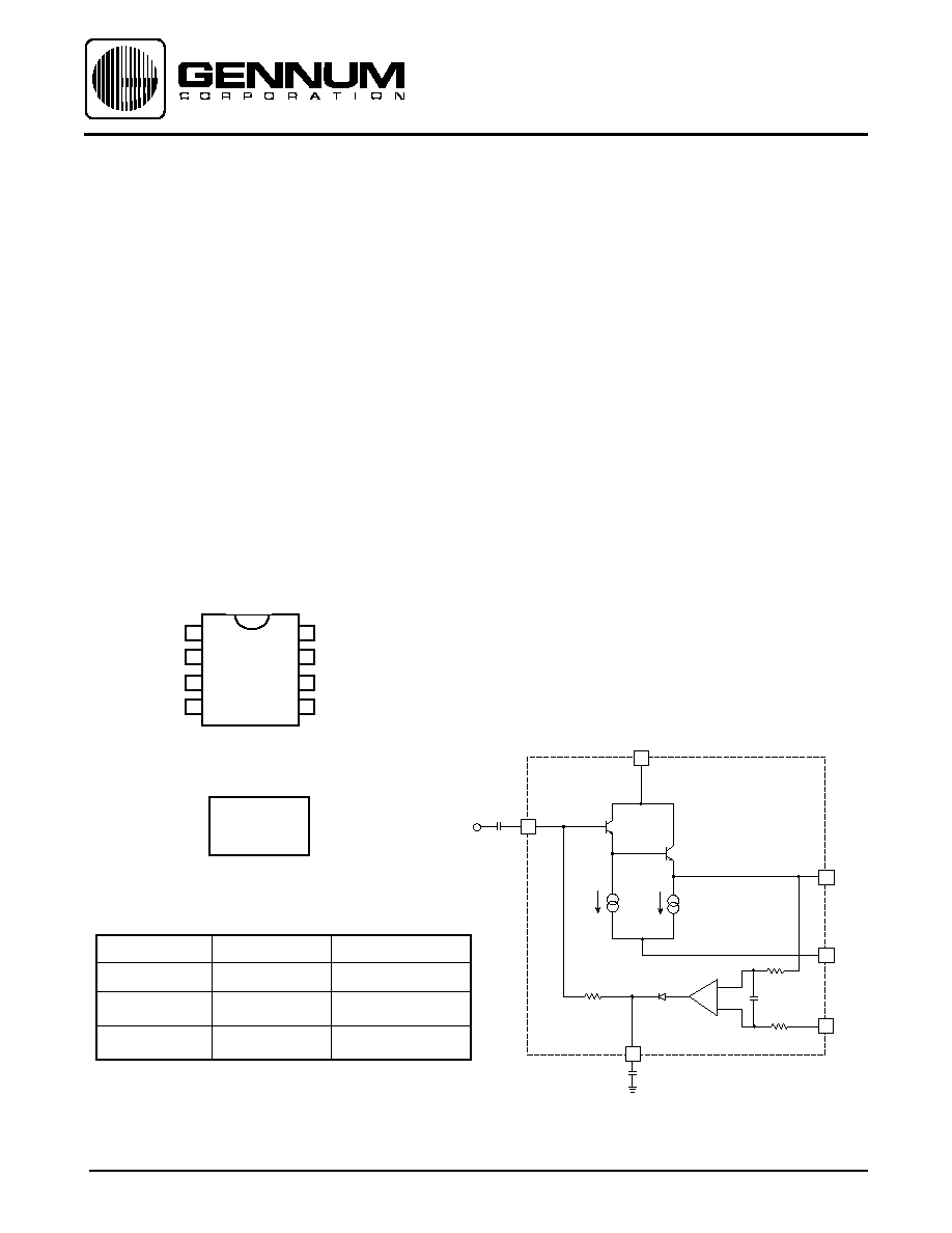
DETAILED DESCRIPTION
The GB4570 is intended for video applications requiring DC
restoration. The GB4570 signal path consists of a wideband
Darlington emitter follower for maximum bandwidth
performance. With this configuration, the GB4570's small
signal frequency response remains within
±
0.1 dB of 0 dB out
to 80 MHz.
Optimal frequency response for the GB4570 occurs with load
capacitance in the range of 15 pF. For smaller loads, an
external capacitor can be added to maximize the bandwidth
of the device. As shown in Figure 1, a small resistor, R
OUT
,
should be included in series with the GB4570 output to obtain
optimal response flatness. For a nominal load of 15 pF, R
OUT
should be chosen to be approximately 40
.
The DC restoration function is achieved through the use of a
simple comparator. The non-inverting input of the comparator
is connected to the clamp reference voltage, while the inverting
input is connected to the GB4570 output. For output signals
more positive than the clamp reference voltage, the comparator
output is essentially open-circuit, while signal voltages more
negative than the clamp reference voltage result in the charging
of C
HOLD
, an external non-polar capacitor connected to pin 4.
The action of the comparator is to provide a positive current
which is fed back to the input under conditions where the
device output is more negative than the clamp reference
voltage. This negative feedback raises the DC level of the
input signal to the point where all signal fluctuations occur at
voltages above the clamp reference voltage.
All resistors are in ohms, all capacitors in microfarads unless otherwise stated
Fig. 1 Typical Application Circuit
75
VIDEO
1.1nF
V
CC
V
EE
8 6
4 1
2 7
3
C
LOAD
C
HOLD
V
CLAMP
V
IN
R
OUT
CLAMPED
VIDEO
OUTPUT
22
0.1
0.1
GB4570
SYNC TIP
CLAMP

4
521 - 18 - 01
C
L
= 82pF
C
L
= 68pF
R
S
= ¯
TYPICAL PERFORMANCE CURVES
10k
-
5V
10
VIDEO OUTPUT
TO NETWORK
ANALYSER I/P
+5V
75
0.1
0.01
GB4570
1 8 6
4 3
C
L
NETWORK
ANALYSER
Sweep: 1-100MHz
Level: 0dBM
0.1
+5V
+5V
4
1
8
5
0.1
0.1
CLC110
R
S
2 7
All resistors are in ohms, all capacitors in microfarads unless otherwise stated
Fig. 2 Frequency Response Test Circuit
6.0
4.0
2.0
0.0
-2.0
GAIN (dB)
1 10 100
FREQUENCY (MHz)
Fig. 3 GB4570 Frequency Response
0.1
0.05
0
-0.05
-0.1
-0.15
-0.2
GAIN (dB)
1
10 100
FREQUENCY (MHz)
Fig. 4 Flattened Frequency Response
R
S
= ¯
1
0
-1
-2
-3
-4
-5
-6
-7
PHASE (deg)
1
10
FREQUENCY (MHz)
Fig. 5 Phase vs Frequency
C
L
= 270pF
C
L
= 180pF
C
L
= 120pF
C
L
= 82pF
1
0
-1
-2
-3
-4
-5
-6
PHASE (deg)
1
10
Fig. 6 Phase vs Frequency
FREQUENCY (MHz)
R
S
= 32
C
L
= 27pF
R
S
= 40
C
L
= 18pF
R
S
= 43
C
L
= 10pF
C
L
= 100pF
C
L
= 120pF
C
L
= 180pF
C
L
= 270pF
R
S
= 32.5
C
L
= 27pF
R
S
= 39
C
L
= 18pF
R
S
= 43
C
L
= 10pF

5
521 - 18 - 01
Gennum Corporation assumes no responsibility for the use of any circuits described herein and makes no representations that they are free from patent infringement.
© Copyright September 1994 Gennum Corporation. All rights reserved. Printed in Canada.
DOCUMENT
IDENTIFICATION
PRODUCT PROPOSAL
This data has been compiled for market investigation purposes
only, and does not constitute an offer for sale.
ADVANCE INFORMATION NOTE
This product is in development phase and specifications are
subject to change without notice. Gennum reserves the right to
remove the product at any time. Listing the product does not
constitute an offer for sale.
PRELIMINARY DATA SHEET
The product is in a preproduction phase and specifications are
subject to change without notice.
DATA SHEET
The product is in production. Gennum reserves the right to make
changes at any time to improve reliability, function or design, in
order to provide the best product possible.