 | –≠–ª–µ–∫—Ç—Ä–æ–Ω–Ω—ã–π –∫–æ–º–ø–æ–Ω–µ–Ω—Ç: GB4600 | –°–∫–∞—á–∞—Ç—å:  PDF PDF  ZIP ZIP |
The GB4600 is a high performance, monolithic unity gain
video buffer made on Gennum's proprietary LSI process.
The device features a stable wideband topology capable
of driving high capacitance video busses.
Optimal system power/bandwidth can be achieved by
using the high/low current mode select (I-SET). In addition,
the GB4600 can be disabled by taking the ENABLE pin to
ground. The ENABLE input is TTL and 5 V CMOS compatible.
The GB4600 operates from ±4.5 to ±5.5 V power supplies
and typically draws 30 mA of current when I-SET is not
connected. The supply current drops by approximately
50% when I-SET is directly connected to V
EE
.
A typical application for the GB4600 is interfacing Gennum's
wide range of video crosspoint switches. The 8 pin SOIC
packaging is ideally suited for space restricted board
∑ Input and output buffering in wide crosspoint matrices
∑ Inter-board video signal buffering
∑ Inter-system video signal buffering
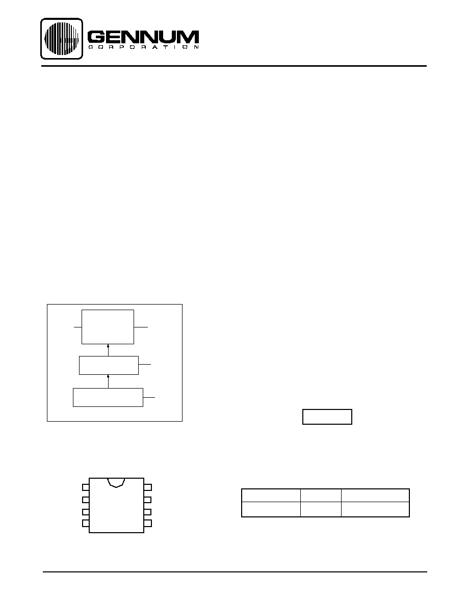
ORDERING INFORMATION
Part Number
Package
Temperature Range
GB4600-CKA
8 SOIC
0∞ to 70∞C
FEATURES
DATA SHEET
∑ wideband, unity gain, stable operation
(
±
0.1 dB at 100 MHz when C
L
= 27 pF)
(full power BW = 120 MHz when C
L
= 47 pF).
∑ selectable high and low current operating
modes (I
L
= 10 mA or I
L
= 20 mA)
∑ drives high capacitance loads (C
L
= 180 pF)
to 70 MHz at -3 dB.
∑ extremely low differential phase and gain
∑ convenient 8 pin SOIC packaging
∑ 100
m
W disabled power consumption
GENNUM CORPORATION P.O. Box 489, Stn A, Burlington, Ontario, Canada L7R 3Y3 tel. (905) 632-2996 fax: (905) 632-5946
Japan Branch: A-302, Miyamae Village, 2-10-42, Miyamae, Suginami-ku, Tokyo 168, Japan tel. (03) 3334-7700 fax. (03) 3247-8839
APPLICATIONS
DESCRIPTION
AVAILABLE PACKAGING
PIN CONNECTIONS
8 pin SOIC
I-SET
NC
INPUT
OUTPUT
3
4
8
5
1
GND
ENABLE
V
EE
2
6
V
CC
7
GB4600 Monolithic
Unity Gain Video Buffer
Document No. 13421 - 5
1
2
3
4
8
7
6
5
Revision Date: February 2003
FUNCTIONAL BLOCK DIAGRAM
VIDEO
SWITCH
ENABLE
INPUT
OUTPUT
ENABLE
CURRENT SET
I-SET
layouts.

2
PARAMETER
VALUE
Supply Voltage
±7.5 V
Operating Temperature Range
0∞C to 70∞C
Storage Temperature Range
-65∞C to 150∞C
Lead Temperature (soldering 10 sec.)
260∞C
Analog Input Voltage
-5.5 V £ V
IN
£ 5.5 V
Logic Input Voltage
-0.5 V £ V
L
£ 5.5 V
ABSOLUTE MAXIMUM RATINGS
PARAMETER
SYMBOL
CONDITIONS
MIN. TYP. MAX. UNITS
Supply Voltage
V
S
±4.5
±5.0
±5.5
V
Supply Current
I+
-
30
37
mA
I-
-
30
37
mA
I+
R-SET = 0 W
-
16
20
mA
I-
R-SET = 0 W
-
16
20
mA
I+ (off)
Enable = 0
-
0
-
mA
I- (off)
Enable = 0
-
16
50
mA
Analog Output Voltage
V
OUT
Unclipped Extremes
-1.8
-
2.2
V
Analog Input Bias Current
IV
BIAS
-
12
-
mA
Output Offset Voltage
V
OS
T
A
= 25∞C
-
5
-
15
mV
Output Offset Voltage Drift
DV
OS
-
50
100
mV/∞C
Chip Enable Time
t
ON
-
100
-
ns
Chip Disable Time
t
OFF
-
1
-
ms
Logic Input Thresholds
V
IH
2.0
-
-
V
V
IL
-
-
0.8
V
Enable Bias Current
I
BIAS
Enable = 0, T
A
= 25∞C
-
-
5.0
m A
Insertion Loss
I.L.
= 100 kHz, T
A
= 25∞C
-
-0.04
-
dB
Frequency Response (±0.1dB)
F.R.
V
IN
= 1 V p-p C
L
= 27 pF
-
100
-
MHz
Full Power (-3dB)
FPBW
V
IN
= 1 V p-p,
-
120
-
MHz
Input Resistance
R
IN
1.0
3.0
-
M W
Input Capacitance
C
IN
-
1.1
-
pF
Output Resistance
R
OUT
-
2
-
W
Output Capacitance
C
OUT
-
5
-
pF
Differential Gain
dg
= 3.58 MHz
-
0.02
-
%
Differential Phase
dp
= 3.58 MHz
-
0.02
-
deg
Off Isolation at 30 MHz
V
IN
= 1 V p-p
75
80
-
dB
+SR
R-SET = 0 (I minimum)
-
250
-
V/ms
V
IN
= 3 V p-p, C
L
= 100 pF
-SR
R
S
= 12 W
-
100
-
V/ms
+SR
V
IN
= 3 V p-p, C
L
= 100 pF
-
350
-
V/ms
-SR
R
S
= 12 W
-
170
-
V/ms
Slew Rate
LOGIC
STATIC
DC
SUPPLY
DYNAMIC
ELECTRICAL CHARACTERISTICS
V
S
= ±5 V, T
A
= 0∞ to 70∞C, R
L
= 10kW, C
L
= 47 pF, R- SET = open circuit unless otherwise shown.
CAUTION
ELECTROSTATIC
SENSITIVE DEVICES
DO NOT OPEN PACKAGES OR HANDLE
EXCEPT AT A STATIC-FREE WORKSTATION
13421 - 5

3
7 4
8 2 5
75
GB4600
3 1
RS
VIDEO INPUT
0.1
5
10 K
-5V
+5V
0.1
CHIP ENABLE
-5V
R
L
Min.
Max.
0.1
-5V
1
+5V
0.1
4
VIDEO OUT
(75 )
10 K
0.1
I-SET
8
CL
W
COMLINEAR
CLC110
The circuit shown above uses the GB4600 as an input
buffer driving several GX4201 video crosspoint ICs.
The GB4600 is capable of driving loads up to 100 pF to
a -3 dB bandwidth of 80 MHz. For lighter loads, the
bandwidth is extended to over 100 MHz.
Capacitor C
L
is used to shape the response in conjunction
with the 27 W series resistor from pin 4. The value shown
will give a -1 dB response at 100 MHz with a total load
capacitance (fixed plus actual) of 47 pF.
In order to disable the GB4600, pin 1 is driven from the
TALLY outputs of the GX4201s. When all crosspoints are
OFF, the voltage on pin 1 will be 0 volts, disabling the
GB4600. Whenever any crosspoint is selected, the
voltage on pin 1 rises to +5 volts and turns on the buffer.
This configuration minimizes the current drain when a
group of crosspoints are turned off.
For other applications, the ENABLE input on the GB4600
may be controlled by any TTL or 5 volt CMOS device.
A unique feature of the GB4600 is that its current drain
can be reduced by adjusting the value of the resistor on
the I-SET input, pin 5.
If R-SET is made zero ohms (a direct connection to -V
EE
)
then the supply current drops 50% from 36 mA to 18 mA.
A reduced current will reduce the bandwidth as shown
in Figure 3. For values of R
S
= 27 W and C
L
= 47 pF, the
-1 dB bandwidth shrinks from 100 MHz at maximum
current to 80 MHz at minimum current.
As with any high frequency circuit, careful board layout
with ample ground plane is critical.
All resistors are in ohms, all capacitors in microfarads unless otherwise stated
All resistors are in ohms, all capacitors in microfarads unless otherwise stated
TEST CIRCUIT
*
The current will be maximum if the pin 5 is left open circuit. Any value of resistance from pin 5 to -V
EE
will reduce the current. The minimum current
(50% of max.) will occur when R-SET
= 0 W.
TYPICAL APPLICATION CIRCUIT
7 4
8 2 5
75
GB4600
3 1
27
VIDEO INPUT
GX4201
0.1
GX4201
GX4201
VIDEO OUT
VIDEO OUT
VIDEO OUT
TALLY OUT
TALLY OUT
TALLY OUT
10K
-5V
-5V
+5V
0.1
CL
*
R-SET
13421 - 5

4
TYPICAL PERFORMANCE CURVES FOR THE GB4600
0.05
0.04
0.03
0.02
0.01
0
1.5
1.0
0.5
0
-0.5
-1.0
-1.5
-2.0
-2.5
-3.0
-3.5
10
200
1
100
V
IN
= 1V p-p
C
L
= 47pF
R
S
= 12W
V
IN
= 1V p-p
R
S
= 18W
C
L
= 100pF
V
BLANKING
= 0V
V
LUMINENCE
= 0.714V
V
IN
= 40 IRE
FREQUENCY (MH
Z
)
Fig. 3 I-SET Bandwidth vs Frequency
Fig. 1 Off - Isolation vs Frequency
1
10
100
300
40
50
60
70
80
90
100
1.5
1.0
0.5
0
-0.5
-1.0
-1.5
-2.0
-2.5
-3.0
-3.5
10
100
200
FREQUENCY (MHz)
dg
dp
dg/dp
100
FREQUENCY (MHz)
1
10
1
3
5
10
FREQUENCY (MHz)
I
SET
= MAX.
I
SET
= MIN.
OFF
ISOLA
TION
(dB)
GAIN
(
d
B)
GAIN
(
d
B)
V
IN
= 1V p-p
R
S
= 27W
R-SET (W)
Fig. 2 Full Power Bandwidth (100 pF) vs Frequency
Fig. 4 Differential Gain and Phase vs Frequency
Fig. 5 SOIC Derating Curves
100 1K 10K 1M
AMBIENT
TEMPERA
TURE
(
o
C)
(STILL
AIR)
80
75
70
65
60
55
50
45
40
V
S
= ±5.0V
V
S
= ±5.3V
V
S
= ±5.5V
DOCUMENT IDENTIFICATION
DATA SHEET
The product is in production. Gennum reserves the right to make
changes at any time to improve reliability, function or design, in
order to provide the best product possible.
Gennum Corporation assumes no responsibility for the use of any circuits described herein and makes no representations that they are free from patent infringement.
© Copyright May 1991 Gennum Corporation. All rights reserved. Printed in Canada.
REVISION NOTES:
13421 - 5
Remove reference to DIP Package.
Remove associated part number from DIP package.