
GENNUM CORPORATION P.O. Box 489, Stn. A, Burlington, Ontario, Canada L7R 3Y3
Tel. +1 (905) 632-2996 Fax. +1 (905) 632-5946 E-mail: info@gennum.com
www.gennum.com
Revision Date: April 2002
Document No. 521 - 33 - 05
NO
T RECOMMENDED
FOR NEW DESIGNS
G
F
91
03
DATA SHEET
FEATURES
FEATURES
FEATURES
FEATURES
∑ 4:2:2 to over-sampled RGB or YC
B
C
R
conversion in a
single device
∑ single 10 bit 4:2:2 input
∑ internal 4:2:2 de-multiplexer
∑ 4:2:2 to 8:8:8 interpolation filters
∑ internal YC
B
CR to RG
B
color space conversion
∑ optional YC
B
C
R
(8:8:8) output mode
∑ setup insertion in Luminance channel under user
control
∑ user selectable digital SIN X/X correction
∑ rounding to 10/8 bit resolution per output channel
∑ 40 MHz maximum clock rate
∑ single +5 V power supply
APPLICATIONS
APPLICATIONS
APPLICATIONS
APPLICATIONS
∑ Over-Sampling 4:2:2 to Analog RGB Conversions for
video monitoring
∑ Over-Sampling 4:2:2 to Analog YCBCR Conversions for
video monitoring
DEVICE DESCRIPTION
DEVICE DESCRIPTION
DEVICE DESCRIPTION
DEVICE DESCRIPTION
The GF9103 is specifically designed to simplify conversions
from 4:2:2 component digital video to analog RGB or
analog YC
B
C
R
component video. The GF9103 simplifies
this process by performing 4:2:2 to 8:8:8 interpolation,
digital color space conversion and digital SIN X/X
correction in a single device. Immediately following the
GF9103, three over-sampled channels of RGB or YC
B
C
R
data may be passed through Digital to Analog converters
and simplified analog reconstruction filters.
The GF9103 accepts a single 10 bit stream of 4:2:2 data
and internally de-multiplexes it into three 10 bit channels of
YC
B
C
R
data. The YC
B
C
R
data is then passed through
three linear phase FIR filters that over-sample the Y data by
a factor of 2 and the C
B
and C
R
data by a factor of 4.
While operating in an over-sampled RGB output mode, the
interpolated YC
B
C
R
data is passed through the internal
color space converter to convert the YC
B
C
R
data to RGB
data according to CCIR-601. Alternatively, the color space
converter may be bypassed to obtain over-sampled YC
B
C
R
(8:8:8) output data. While operating in YC
B
C
R
output mode,
setup may be dynamically inserted into the Luminance
channel.
Prior to output rounding, over-sampled YC
B
C
R
or RGB data
may be corrected for SIN X/X characteristics of D/A
conversion. Output data may be rounded to 10 or 8 bit
resolution per channel. C
B
and C
R
may be presented as
signed or unsigned data.
The GF9103 is packaged in a 68 pin PLCC package,
operates with a single +5 V power supply and typically
consumes only 85 mA of current when operated at 27 MHz.
FUNCTIONAL BLOCK DIAGRAM
FUNCTIONAL BLOCK DIAGRAM
FUNCTIONAL BLOCK DIAGRAM
FUNCTIONAL BLOCK DIAGRAM
ORDERING INFORMATION
ORDERING INFORMATION
ORDERING INFORMATION
ORDERING INFORMATION
PART NUMBER
PACKAGE
TEMPERATURE RANGE
GF9103-CPS
68 pin PLCC
0∞ to 70∞ C
GF9103-CTS
68 pin PLCC Tape
0∞ to 70∞ C
10
10
10
CLIP & ROUND
CLIP & ROUND
CLIP & ROUND
SELECT_MATRIX
SETUP
SETUP
SIN X/X
SIN X/X
SIN X/X
Y
MULTIPLEXED
4:2:2 DATA
STREAM IN
YCBCR
TO
RGB
MATRIX
BYPASS
CB
4:2:2
DEMUX
SYNC
CLK
OE
CR
Y
X2
X4
X4
CB
CR
CR
Y
CB
Y/G
CR/R
CB/B
Y/G
CB/B
CR/R
Y/G
CB/B
CR/R
Y/G
CB/B
CR/R
CB/B
CR/R
2's COMP
CONVERT
2's COMP
10
0XOWLGEN
TM
GF9103 Over-Sampling
GF9103 Over-Sampling
GF9103 Over-Sampling
GF9103 Over-Sampling
Color Space Converter for
Color Space Converter for
Color Space Converter for
Color Space Converter for
Video Monitoring
Video Monitoring
Video Monitoring
Video Monitoring
521 - 33 - 05
2
NO
T RECOMMENDED
FOR NEW DESIGNS
G
F
91
03
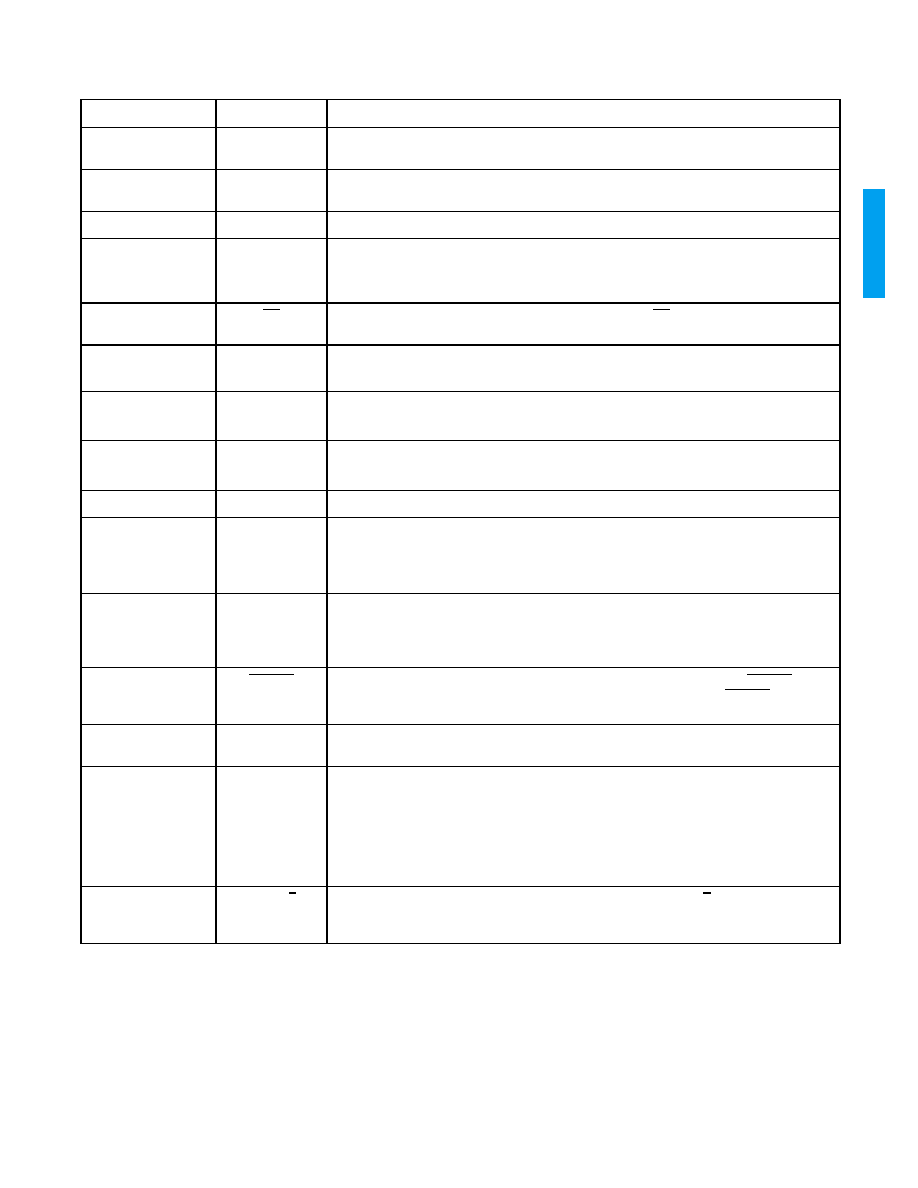
PIN DESCRIPTION
PIN DESCRIPTION
PIN DESCRIPTION
PIN DESCRIPTION
PIN NO.
SYMBOL
DESCRIPTION
10, 18, 27, 36, 44, 52,
61, 68
V
DD
±5 V ± 5% power supply.
1, 6, 7, 9, 26, 30, 35,
40, 43, 60, 64
GND
Ground.
3
SCAN_EN
Set Low.
8, 11-17, 19, 20
SI
9..0
Input Data Port: Input data port with internal pull-downs. Input data is assumed to be a
multiplexed stream of C
B
YC
R
[Y] C
B
..., where [Y] denotes an isolated Luminance sample.
SI
9
is the Most Significant Bit and SI
0
is the Least Significant Bit.
4
OE
Output Enable: Active low input with internal pull-up. When OE is high, the output data ports
are in high impedance state.
59-53, 51-49
SOA
9..0
Output Data Port A: Depending on device configuration, SOA
9..0
may output over-sampled
Y or G video. SOA
9
is the Most Significant Bit and SOA
0
is the Least Significant Bit.
48-45, 42, 41, 39-37,
34
SOB
9..0
Output Data Port B: Depending on device configuration, SOB
9..0
may output over-sampled
C
B
or B video. SOB
9
is the Most Significant Bit and SOB
0
is the Least Significant Bit.
33-31, 29, 28, 25-21
SOC
9..0
Output Data Port C: Depending on device configuration, SOC
9..0
may output over-sampled
C
R
or R video. SOC
9
is the Most Significant Bit and SOC
0
is the Least Significant Bit.
2
CLK
System Clock: All timing information relative to rising edge of clock.
5
SYNC
Synchronization: Control signal input with internal pull-up. This input is used to synchronize
the incoming data by holding SYNC high on clock period N and low on clock period N+1
when the first C
B
sample is presented to the SI
9..0
inputs. SYNC may be held low until re-
synchronization is desired or may be toggled at every occurrence of a C
B
sample.
65
SELECT_MATRIX
Select Color Space Conversion: Control signal input with internal pull-down.
SELECT_MATRIX is used to enable and disable the internal YC
B
C
R
to RGB color space
converter. Color space conversion is enabled while SELECT_MATRIX is high and is
disabled while SELECT_MATRIX is low.
66
BYPASS
Bypass SIN X/X Correction: Control signal input with internal pull-up. When BYPASS is
high, SIN X/X correction for the three output channels is enabled. While BYPASS is low, SIN
X/X correction is by-passed.
63
SETUP
Setup: Control signal input with internal pull-down. SETUP is used to enable and disable
setup insertion in the Luminance channel.
62
CONVERT
Two's Complement Conversion: Control signal input with internal pull-up. While CONVERT
is high, SOB
9..0
and SOC
9..0
output signed (two's complement) digital data. While
CONVERT is low, SOB
9..0
and SOC
9..0
output unsigned (offset binary) data. When
operating in RGB output mode, the CONVERT pin is over-ridden and both SOB
9..0
and
SOC
9..0
output unsigned digital data. SOA
9..0
outputs unsigned digital data in all operating
modes.
67
RND10/8
Output Rounding: Control signal input with internal pull-up. RND10/8 selects rounding to
10 bit resolution per channel when high and rounding to 8 bit resolution per channel when
low.

521 - 33 - 05
3
NO
T RECOMMENDED
FOR NEW DESIGNS
G
F
91
03
Fig. 1 GF9103 Pin Connections
Fig. 2a Equivalent Input Circuit
Fig. 2b Equivalent Output Circuit
GND
SOA9
SOA8
SOA7
SOA6
SOA5
SOA4
SOA3
VDD
SOA2
SOA1
SOA0
SOB9
SOB8
SOB7
SOB6
VDD
VDD
SI8
SI7
SI6
SI5
SI4
SI3
SI2
VDD
SI1
SI0
SOC0
SOC1
SOC2
SOC3
SOC4
GND
VDD
SOC5
SOC6
GND
SOC7
SOC8
SOC9
SOB0
GND
VDD
SOB1
SOB2
SOB3
GND
SOB4
SOB5
GND
GND
SI9
GND
GND
SYNC
OE
SCAN_EN
CLK
GND
VDD
RND10/8
BYPASS
SELECT_MATRIX
GND
SETUP
CONVERT
VDD
GF9103
TOP VIEW
60
59
58
57
56
55
54
53
52
51
50
49
48
47
46
45
44
10
11
12
13
14
15
16
17
18
19
20
21
22
23
24
25
26
27 28 29 30 31 32 33 34 35 36 37 38 39 40 41 42 43
9 8 7 6 5 4 3 2 1 68 67 66 65 64 63 62 61
n SUBSTRATE
CONTROL
INPUT
p WELL
GND
n
p
VDD
D1
D2
n+
p+
D1
D2
GND
n SUBSTRATE
p WELL
n
p
n+
p+
VDD

521 - 33 - 05
4
NO
T RECOMMENDED
FOR NEW DESIGNS
G
F
91
03
DEVICE DESCRIPTION
DEVICE DESCRIPTION
DEVICE DESCRIPTION
DEVICE DESCRIPTION
The GF9103 is composed of five main sections:
1. 4:2:2 De-Multiplexer
2. FIR Filtering and Setup Insertion
3. Color Space Conversion
4. Digital SIN X/X Correction
5. Output Processing
4:2:2 DE-MULTIPLEXER
4:2:2 DE-MULTIPLEXER
4:2:2 DE-MULTIPLEXER
4:2:2 DE-MULTIPLEXER
The de-multiplexer accepts data multiplexed in a SMPTE
125M compliant format from the
SI9..0
input data port.
SI9
is
the Most Significant Bit and
SI0
is the Least Significant Bit.
The input data stream is assumed to be a multiplexed
stream of C
B
Y C
R
[Y] C
B
..., where the three words C
B
Y C
R
refer to cosited samples and where [Y] refers to an isolated
Luminance sample. When operating the GF9103 with 8 bit
input data,
SI9..2
should be used to present data to the
device and
SI1..0
should be set low.
At least once during a power cycle, the GF9103 must be
synchronized to the incoming data stream. The GF9103 is
synchronized by holding SYNC high on clock period N and
low on clock period N+1 when the first C
B
sample is
presented to the
SI9..0
inputs. SYNC may be held low until
re-synchronization is desired, or it may be toggled at every
occurrence of a C
B
sample. Refer to the timing diagram in
Figure 9 for required operation of the SYNC control signal.
The internal de-multiplexer will de-multiplex all data in the
input data stream including any ancillary, EDH,VITC, and
EAV/SAV ... signals that may be present. Since this data is
passed directly to the interpolation filters in the same way
that active video would be, it is recommended that such
data be replaced with appropriate blanking levels prior to
entering the GF9103.
The output of the 4:2:2 de-multiplexer consists of three 10
bit channels of YC
B
C
R
data. All three channels are then fed
to their respective interpolation filter.
INTERPOLATION FILTERS
INTERPOLATION FILTERS
INTERPOLATION FILTERS
INTERPOLATION FILTERS
Within the interpolation stage, the Luminance data is over-
sampled by a factor of two and the C
B
and C
R
data is over-
sampled by a factor of four so that the 4:2:2 data is
converted to 8:8:8 data. By over-sampling the 4:2:2 data to
8:8:8 data, the size, cost and complexity of the analog
reconstruction filters following Digital to Analog converters
are reduced.
The Luminance data is over-sampled by a linear phase FIR
filter providing 0.0 dB DC gain, +0.038/-0.025 pass- band
ripple [0.0 s to 0.21 s], 6 dB attenuation at s/4, and 47
dB stopband attenuation [0.30 s to 0.50 s]. Figure 3 and
Figure 4 present the frequency response of the Luminance
interpolation filter.
The C
B
and C
R
data is over-sampled by a linear phase FIR
filter providing 0.0 dB DC gain, passband ripple of +0.2 dB/-
0.2 dB [0.0 to 0.07 s], 6 dB attenuation at s/8 and a
stopband attenuation of 28 dB [ 0.17s to 0.50 s].
Figure 5 and Figure 6 present the frequency response of the
C
B
and C
R
interpolation filters.
Following the interpolation process, a DC offset may be
introduced into the Luminance channel. Setup insertion is
enabled and disabled by the SETUP control signal. While
SETUP is high, the Luminance data is scaled by a factor of
+947/1024 and an offset of +71 (decimal) is added. While
SETUP is low, no scaling or offset is applied and the data
passes through the stage unmodified. The timing diagram
in Figure 10 demonstrates the operation of the SETUP
control signal.
COLOR SPACE CONVERSION
COLOR SPACE CONVERSION
COLOR SPACE CONVERSION
COLOR SPACE CONVERSION
Two operating modes exist for the color space converter
section. These two modes are controlled by the
SELECT_MATRIX control signal. While SELECT_MATRIX is
low, the de-matrixing 3 x 3 multiplier is bypassed so that
over-sampled Y C
B
C
R
data is passed through the stage
unmodified. While SELECT_MATRIX is high, the 3 x 3
multiplier implements the following color space conversion:
SIN X/X CORRECTION
SIN X/X CORRECTION
SIN X/X CORRECTION
SIN X/X CORRECTION
While BYPASS is high, SIN X/X correction is enabled on
each of the three output channels. SIN X/X correction is
implemented by passing the data through a FIR filter with
the frequency response shown in Figure 7. While BYPASS is
low, the FIR filter is bypassed and each channel is passed
directly to the output processing section. Total latency
through the device is 22 clock cycles when BYPASS is low
and 24 clock cycles when BYPASS is high.
OUTPUT PROCESSING
OUTPUT PROCESSING
OUTPUT PROCESSING
OUTPUT PROCESSING
Output data may be rounded to 10 or 8 bit accuracy.
RND10/8
should be set high for 10 bit output rounding and
set low for 8 bit output rounding. Rounding to 8 bit accuracy
is accomplished by adding a rounding bit to SO
1
and then
zeroing both SO
0
and SO
1
.
C
B
and C
R
data may be output as signed (two's
complement) or unsigned (offset binary) data depending on
the state of the CONVERT control signal. When CONVERT
is set high, the C
B
and C
R
channels are output as signed
(two's complement) data. When CONVERT is set low, C
B
and C
R
are output as unsigned (offset binary) data,
obtained by inverting the sign bit of the two's complement
number. When operating in RGB output mode, the
CONVERT pin is over-ridden and RGB data is always
output as unsigned (offset binary) data.
G
B
R
1
-689/2048
-1430/2048
1
3548/2048
0
1
0
2807/2048
Y
C
B
C
R
=

521 - 33 - 05
5
NO
T RECOMMENDED
FOR NEW DESIGNS
G
F
91
03
CONTROL SIGNAL/OPERATING MODE SUMMARY
CONTROL SIGNAL/OPERATING MODE SUMMARY
CONTROL SIGNAL/OPERATING MODE SUMMARY
CONTROL SIGNAL/OPERATING MODE SUMMARY
SYNC
SYNC
SYNC
SYNC
The SYNC control signal provides synchronization for the internal 4:2:2 de-multiplexer. SYNC should be held high on clock
period N and low on clock period N+1 when the first C
B
sample is presented to the SI
9..0
inputs. SYNC may be held low until
re-synchronization is desired or may be toggled at every occurrence of a C
B
sample.
SELECT_MATRIX AND SETUP
SELECT_MATRIX AND SETUP
SELECT_MATRIX AND SETUP
SELECT_MATRIX AND SETUP
SELECT_MATRIX and SETUP select the color space conversion and offset insertions which the GF9103 is to perform. The
following chart presents the available color space conversions and the corresponding states of the SELECT_MATRIX and
SETUP control pins. SETUP is a dynamic pin that may be modified every clock cycle.
SELECT_MATRIX
SETUP
DESCRIPTION
0
0
Selects output to be over-sampled YC
B
C
R
with no setup in Y channel.
0
1
Selects output to be over-sampled YC
B
C
R
with a scaling factor of
+947/1024 and an offset of +71 (decimal) applied to the Y channel.
1
X
Selects output to be over-sampled RGB with no setup.
SIN X/X CORRECTION
SIN X/X CORRECTION
SIN X/X CORRECTION
SIN X/X CORRECTION
BYPASS
DESCRIPTION
1
SIN X/X correction enabled on all output data channels. Latency through the device is 24 clock cycles.
0
SIN X/X correction disabled. Latency through the device is 22 clock cycles.
OUTPUT ROUNDING
OUTPUT ROUNDING
OUTPUT ROUNDING
OUTPUT ROUNDING
RND10/8
DESCRIPTION
1
Output data rounded to 10 bit resolution per channel.
0
Output data rounded to 8 bit resolution per channel.
TWO'S COMPLEMENT OUTPUT CONVERSION
TWO'S COMPLEMENT OUTPUT CONVERSION
TWO'S COMPLEMENT OUTPUT CONVERSION
TWO'S COMPLEMENT OUTPUT CONVERSION
CONVERT
SELECT_MATRIX
DESCRIPTION
1
0
SOB
9..0
and SOC
9..0
output signed (two's complement) C
B
and C
R
data.
0
0
SOB
9..0
and SOC
9..0
output unsigned (offset binary) C
B
and C
R
data.
X
1
SOB
9..0
and SOC
9..0
output unsigned B and R data.
OUTPUT ENABLE
OUTPUT ENABLE
OUTPUT ENABLE
OUTPUT ENABLE
OE
DESCRIPTION
0
All output data ports are enabled.
1
All output data ports are in high impedance state.