www.gennum.com
GF9331 HDTV/SDTV
Motion Co-processor
GF9331 Data Sheet
Proprietary and Confidential
18303 - 4
June 2004
1 of 31
Features
∑
support for 10/8-bit HDTV/SDTV input video signals
∑
seamless interface to Gennum's GF9330 high
performance de-interlacer through a filter control bus
∑
multi-directional edge detection and control
∑
support for multiplexed and non-multiplexed Y/C video
∑
3-field vertical motion detection and control
∑
fully configurable to support custom video modes
∑
ability to extract HVF information from embedded TRS
∑
seamless interface to popular ADCs and NTSC/PAL
decoders
∑
user configuration through a dedicated host interface,
supporting parallel and serial interfaces
∑
5V tolerant inputs
∑
3.3V supply for device I/O and 2.5V for core logic
Applications
∑
HDTV Up/Down Converters
∑
Production Equipment
∑
Video Walls
∑
Projection Systems
∑
Plasma Displays
∑
LCD TVs
∑
Home Theatre Systems
∑
HD DVD Players
Device Overview
The GF9331 is a high performance motion
co-processor that is used in conjunction with Gennum's
GF9330 HDTV/SDTV 10-bit De-interlacer. Together,
the GF9331 and the GF9330 provide 10-bit broadcast
quality de-interlacing for standard and high-definition
video signals up to 1080p60.
Although the GF9330 can fully function as a stand alone
de-interlacer, the GF9331 provides added features in
the form of a filter selection control bus that enables
multi-directional edge and adaptive 3-field vertical
motion detection. Edge detection and interpolation
removes the edge artifacts that tend to occur while
de-interlacing on shallow horizontal edges while vertical
motion detection reduces motion artifacts.
Filter selection controls are sent to the GF9330 on a
pixel-by-pixel basis. The GF9331 integrates all the
necessary line delays for the motion and edge
detectors. The GF9331 also provides seamless
interfaces to off-chip SDRAMs that form the required
field delays.
Ordering Information
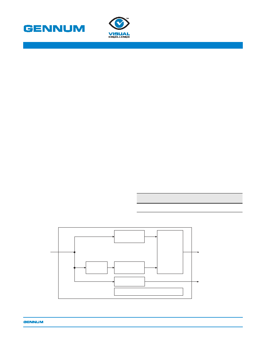
Block Diagram
Part Number
Package
Temp. Range
GF9331-CBP
328 PIN BGA
0
o
C to 70
o
C
Pre-filter
Encoder
Edge Detection
Vertical Motion
Detection
Y/C
Control bus
to GF9330
External Memory Interface
Delay
Y/C Delayed Video
to GF9330

GF9331 Data Sheet
Proprietary and Confidential
18303 - 4
June 2004
2 of 31
Contents
Features ........................................................................................................................1
Applications...................................................................................................................1
Device Overview ...........................................................................................................1
Ordering Information .....................................................................................................1
1. Pin Descriptions ........................................................................................................3
2. Electrical Characteristics...........................................................................................7
2.1 5V Tolerant Inputs ...........................................................................................7
2.2 ESD Tolerance ................................................................................................7
2.3 3.3V Supply for Device I/0 and 2.5V for Core Logic .......................................7
3. Detailed Device Description ....................................................................................10
3.1 Input Data Formats .......................................................................................10
3.2 Input Synchronization ...................................................................................12
3.2.1 Support for Both 8-bit and 10-bit Input Data ........................................12
3.2.2 Generic Input Format Signalling ..........................................................12
3.3 Seamless Interface to the GF9330 High Performance De-Interlacer for
Directional Filter Control ...............................................................................15
3.4 Seamless Interface to External SDRAMs .....................................................16
3.5 Host Interface ................................................................................................16
3.5.1 Host Interface Serial Mode ..................................................................17
3.5.2 Host Interface Parallel Mode ...............................................................20
3.5.3 Control Register Definitions .................................................................23
3.6 Closed Captioning .........................................................................................25
3.7 RESET ..........................................................................................................25
3.8 Modes of Operation ......................................................................................25
3.8.1 Motion Processing Mode (MODE=1) ...................................................26
3.8.2 Disabled Mode (MODE=0)...................................................................26
3.9 Processing of Input Formats .........................................................................26
3.10 Vertical Motion Detection ............................................................................28
3.10.1 Vertical Motion Feature Control .........................................................28
3.11 Edge Direction Detection ............................................................................28
3.11.1 Edge Direction Detection Feature Control .........................................29
3.12 Video Output ...............................................................................................29
3.13 Processing Latency .....................................................................................29
4. Package Dimensions ..............................................................................................30
5. Revision History ......................................................................................................31
GF9331 Data Sheet
Proprietary and Confidential
18303 - 4
June 2004
3 of 31
1. Pin Descriptions
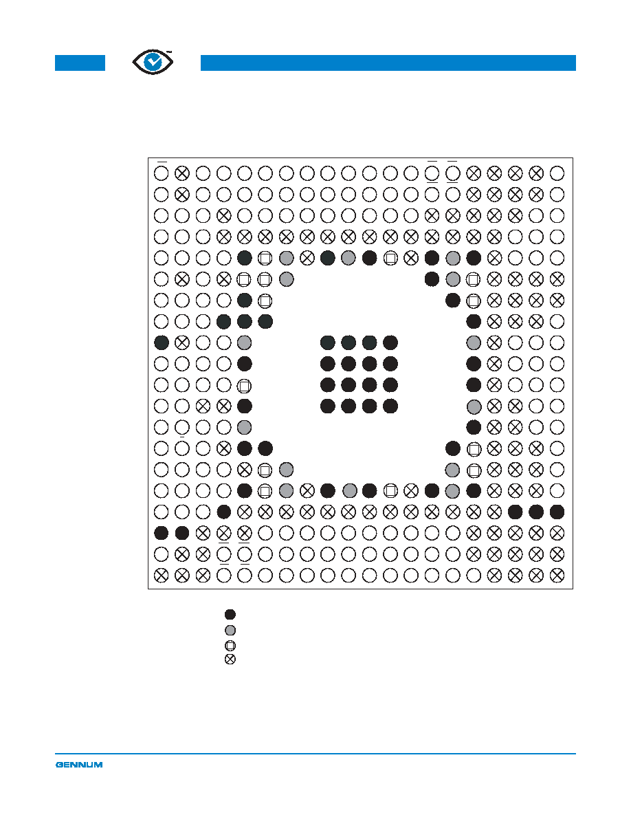
Figure 1-1: Top View Pin Out (328-pin BGA)
A
B
C
D
J
K
E
F
G
H
L
M
N
P
W
Y
R
T
U
V
1
2
3
4
5
6
7
8
9
10 11 12 13 14 15 16 17 18 19 20
RESET
Y_IN9
NC
NC
Y_IN8
Y_IN5
Y_IN7
Y_IN4
S2_DAT0
S2_DAT1
S2_DAT2
S2_DAT3
Y_IN6
Y_IN3
NC
NC
S2_DAT4
S2_DAT5
S2_DAT7
S2_DAT8
S2_DAT6
NC
S2_DAT9
NC
S2_DAT10
S2_DAT11
S2_DAT13
S2_DAT14
S2_DAT12
NC
S2_DAT15
NC
S2_CLK
S2_ADDR0
S2_ADDR2
S2_ADDR3
S2_ADDR1
NC
S2_ADDR4
NC
S2_ADDR7
S2_ADDR6
S2_ADDR10
S2_ADDR9
S2_ADDR5
NC
S2_ADDR8
NC
S2_ADDR13
S2_ADDR12
S2_CS
S2_CAS
S2_ADDR11
NC
NC
NC
S2_WE
S2_RAS
NC
NC
NC
NC
NC
NC
NC
NC
NC
NC
NC
NC
NC
Y_OUT3
NC
NC
Y_OUT9
Y_OUT8
Y_OUT6
Y_OUT4
Y_OUT7
Y_OUT5
Y_IN2
VCLK_IN
Y_IN1
NC
SER_MD
MEMCLK_IN
STD4
STD1
Y_IN0
MODE
HOST_EN
NC
STD3
STD0
STD2
GND
VDD_CLKD
VDD_INT
VDD_INT
VSS_CLKD
GND
VDD_INT
GND
VDD_IO
VDD_IO
NC
GND
VDD_IO
GND
VDD_INT
NC
GND
GND
VDD_IO
VDD_IO
GND
VDD_INT
GND
VDD_INT
GND
NC
NC
NC
NC
NC
NC
NC
Y_OUT1
NC
Y_OUT2
NC
NC
NC
NC
C_OUT9
C_IN7
NC
C_IN6
C_IN0
ED_MODE
C_IN1
VM_MODE
C_IN9
C_IN5
C_IN8
C_IN4
C_IN2
NC
C_IN3
NC
VDD_IO
GND
VDD_INT
GND
TGND
TGND
TGND
TGND
TGND
TGND
TGND
TGND
TGND
TGND
TGND
TGND
TGND
TGND
TGND
TGND
VDD_IO
GND
GND
VDD_IO
NC
NC
C_OUT6
C_OUT3
NC
NC
C_OUT2
NC
C_OUT7
C_OUT4
C_OUT8
C_OUT5
C_OUT1
FIL_SEL3
C_OUT0
FIL_SEL2
FVH_EN
A_D
F_IN
CS
DAT_IO4
DAT_IO0
DAT_IO5
DAT_IO1
V_IN
R_W
H_IN
NC
DAT_IO6
DAT_IO2
DAT_IO7
DAT_IO3
VDD_IO
GND
GND
NC
GND
VDD_INT
VDD_INT
VDD_IO
VDD_IO
NC
GND
VDD_IO
GND
VDD_INT
NC
GND
GND
GND
VDD_INT
VDD_IO
VDD_IO
VDD_INT
GND
NC
NC
NC
NC
NC
NC
NC
NC
FIL_SEL1
NC
FIL_SEL0
H_OUT
NC
NC
V_OUT
F_OUT
TCLK
GND
TMS
GND
TDO
NC
NC
NC
TDI
NC
GND
NC
NC
NC
S1_RAS
S1_WE
NC
NC
NC
S1_ADDR11
S1_CAS
S1_CS
S1_ADDR12
S1_ADDR13
NC
S1_ADDR8
NC
S1_ADDR5
S1_ADDR9
S1_ADDR10
S1_ADDR6
S1_ADDR7
NC
S1_ADDR2
NC
S1_ADDR0
S1_ADDR3
S1_ADDR4
S1_ADDR1
S1_CLK
NC
S1_DAT15
NC
S1_DAT12
S1_DAT14
S1_DAT13
S1_DAT11
S1_DAT10
NC
S1_DAT9
NC
S1_DAT6
S1_DAT8
S1_DAT7
S1_DAT5
S1_DAT4
NC
S1_DAT3
NC
NC
S1_DAT2
S1_DAT1
NC
S1_DAT0
NC
NC
GND
NC
NC
NC
NC
NC
GND
NC
GND
NC
NC
NC
NC
NC
Y_OUT0
TOP VIEW
GF9331 PIN OUT
328 BGA
GND/TGND: 0V
NC: No Connection
VDD_IO: +3.3V
VDD_INT: +2.5V
GND
GND

GF9331 Data Sheet
Proprietary and Confidential
18303 - 4
June 2004
4 of 31
Table 1-1: Pin Descriptions
Symbol
Pin Grid
Type
Description
RESET
A1
I
Active low, asynchronous RESET. Resets all internal logic to default
conditions. Should be applied on power up.
VCLK_IN
F1
I
Video input clock. When the input is SDTV the input clock will be 27, 36, 54 or
72MHz. When the input format is HDTV, the input clock will be 74.25 or
74.25/1.001MHz.
MEMCLK_IN
H1
I
Memory clock for SDRAM operation when VLCK_IN > 36MHz. 90MHz input
(supplied by an off-chip crystal oscillator).
Y_IN[9:0]
B1, C1, C2, C3, D1, D2,
D3, E1, E2, E3
I
8/10-bit input data bus for separate luminance or multiplexed luminance and
colour difference video data. When supplying 8-bit data to the GF9331,
Y_IN[1:0] will be set LOW and the 8-bit data supplied to Y_IN[9:2].
C_IN[9:0]
J3, J4, K1, K2, K3, K4, L4,
L3, L2, L1
I
8/10-bit input data bus for colour difference video data. When supplying 8-bit
data to the GF9331, C_IN[1:0] will be set LOW and the 8-bit data supplied to
C_IN[9:2].
F_IN
N2
I
Video timing control. F_IN identifies the ODD and EVEN fields in the incoming
video signal. F_IN will be LOW in Field 1 and HIGH in Field 2.
V_IN
N3
I
Video timing control. V_IN represents the vertical blanking signal associated
with the incoming video signal. V_IN is HIGH during the vertical blanking
interval and LOW during active video.
H_IN
N4
I
Video timing control. H_IN represents the horizontal blanking signal
associated with the incoming video signal. H_IN is HIGH during horizontal
blanking and LOW during active video.
FVH_EN
N1
I
Control signal input. When HIGH, the F_IN, V_IN, and H_IN input pins will be
used for video data signalling. When LOW, embedded TRS's will be detected
for video data signalling.
VM_MODE
M2
I
Control signal input. When HIGH, the vertical motion detection is enabled.
ED_MODE
M1
I
Control signal input. When HIGH, the edge direction detection is enabled.
STD[4:0]
G2, G3, G4, H2, H3
I
Video format definition. Defines the video standard when operating without the
host interface. See
Table 3-1: Encoding of STD[4:0] for Selecting Input Data
Format
. STD[4:0] is read into the device on a falling transition of HOST_EN or
after a RESET.
MODE
F3
I
Operating mode selection. When HIGH, the GF9331 motion co-processing is
enabled. When LOW, the GF9331 motion co-processing is bypassed. See
Modes of Operation
. MODE is read into the device on a falling transition of
HOST_EN or after a RESET.
HOST_EN
E4
I
Host interface enable. When set HIGH, the GF9331 is configured through the
host interface. When set LOW, the GF9331 is manually configured via input
pins. These values are loaded in on the falling transition of HOST_EN.
SER_MD
G1
I
Host interface mode selection. Enables serial mode operation when HIGH.
Enables parallel mode operation when LOW.
CS
P2
I
Functions as an active low chip select input for host interface parallel mode
operation. Functions as a serial clock input for host interface serial mode
operation.
DAT_IO[7:0]
R4, R3, R2, R1, T4, T3,
T2, T1
I/O
Host interface bi-directional data bus for parallel mode. In serial mode,
DAT_IO[7] serves as the serial data output pin and DAT_IO[0] serves as the
serial data input pin.

GF9331 Data Sheet
Proprietary and Confidential
18303 - 4
June 2004
5 of 31
R_W
P3
I
Host interface Read/Write control for parallel mode. A read cycle is defined
when HIGH, a write cycle is defined when LOW.
A_D
P1
I
Host interface Address/Data control for parallel mode. The data bus contains
an address when HIGH, a data word when LOW. In serial mode, this pin
serves as the chip select (active low).
Y_OUT[9:0]
A20, B20, C20, C19, D20,
D19, D18, E20, E19, E18
O
Output data bus for separate luminance or multiplexed luminance and colour
difference video data.
C_OUT[9:0]
H20, J20, J19, J18, K20,
K19, K18, L18, L19, L20
O
Output data bus for colour difference video data.
FIL_SEL[3:0]
M19, M20, N19, N20
O
Filter selection control bus output to the GF9330. The FIL_SEL[3:0] bus is
used to switch the GF9330's internal directional filters on a pixel by pixel basis.
H_OUT
P20
O
Output control signal. H_OUT is a horizontal blanking output.
F_OUT
T20
O
Output control signal. F_OUT is an ODD/EVEN field indicator.
V_OUT
R20
O
Output control signal. V_OUT is a vertical blanking output.
S1_CLK
Y10
O
SDRAM bank 1 clock.
S1_CS
Y5
O
Active low SDRAM chip select for Field Buffer 1.
S1_RAS
W4
O
Active low SDRAM row address strobe for Field Buffer 1.
S1_CAS
W5
O
Active low SDRAM column address strobe for Field Buffer 1.
S1_WE
Y4
O
Active low SDRAM write enable for Field Buffer 1.
S1_ADDR[13:0]
Y6, W6, V6, Y7, W7, V7,
Y8, W8, V8, Y9, W9, V9,
W10, V10
O
SDRAM address for Field Buffer 1.
S1_DAT[15:0]
V11, W11, Y11, V12, W12,
Y12, V13, W13, Y13, V14,
W14, Y14, V15, W15, Y15,
Y16
I/O
SDRAM data for Field Buffer 1.
S2_CLK
A9
O
SDRAM bank 2 clock.
S2_CS
A14
O
Active low SDRAM chip select for Field Buffer 2.
S2_RAS
B15
O
Active low SDRAM row address strobe for Field Buffer 2.
S2_CAS
B14
O
Active low SDRAM column address strobe for Field Buffer 2.
S2_WE
A15
O
Active low SDRAM write enable for Field Buffer 2.
S2_ADDR[13:0]
A13, B13, C13, A12, B12,
C12, A11, B11, C11, C10,
B10, A10, C9, B9
O
SDRAM address for Field Buffer 2.
S2_DAT[15:0]
C8, B8, A8, C7, B7, A7,
C6, B6, A6, C5, B5, A5,
B4, A4, B3, A3
I/O
SDRAM data for Field Buffer 2.
TDI
U3
I
JTAG data input; connect to GND if not used.
TMS
U2
I
JTAG mode select; connect to GND if not used.
Table 1-1: Pin Descriptions (Continued)
Symbol
Pin Grid
Type
Description