 | –≠–ª–µ–∫—Ç—Ä–æ–Ω–Ω—ã–π –∫–æ–º–ø–æ–Ω–µ–Ω—Ç: GH580 | –°–∫–∞—á–∞—Ç—å:  PDF PDF  ZIP ZIP |
A OUT
R
CNT
CP+
GND
A IN
V
B
A
CONTROL
8
5
6
3
4
7
1
+
_
CP-
1n
1n
V
REG
+
+
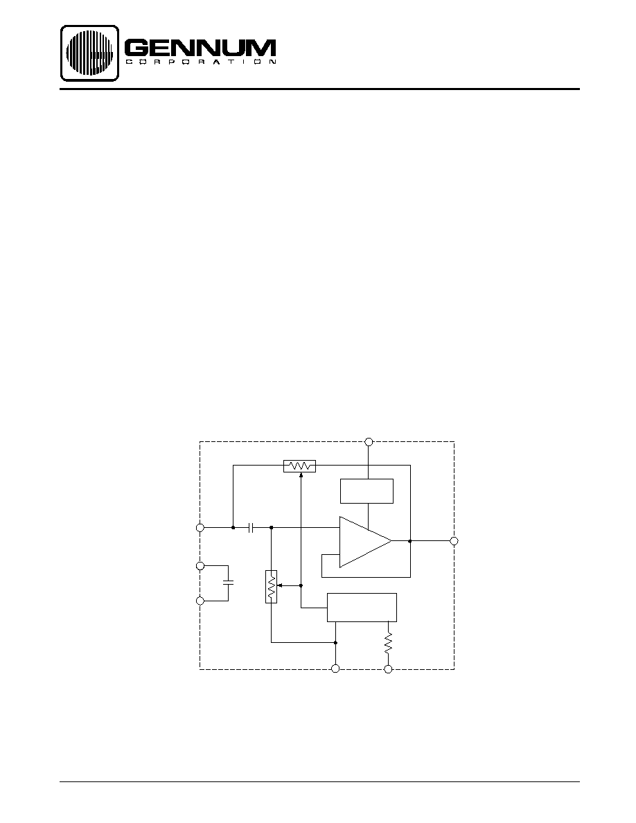
BLOCK DIAGRAM
GH580 - DATA SHEET
∑
200 to 8 kHz adjustable corner frequency
∑
12 dB/oct Butterworth filter
∑
low current drain (175
µ
A typical)
∑
two on chip 1 nF capacitors
∑
low noise and distortion
∑
1.1 to 3.0 VDC operation
STANDARD PACKAGING
∑ 8 pin PLID
Æ
∑ Chip (66 x 61 mils)
FEATURES
DESCRIPTION
The GH580 is a single, second order (12 dB/Oct) continuous
high pass filter with an adjustable corner frequency (
C
) from
200 to 8 kHz. Adjustment of
C
is accomplished with a single
100 k
potentiometer connected from pin 3 to ground.
The bias circuitry is operated from an on chip voltage regulator
providing good supply rejection down to 1.1 V.
The two integrated 1 nF capacitors have parasitic diodes
connected in parallel. This necessitates that the DC voltage
at pin 6 be greater that 400 mV and less than VB and that pins
8 and 7 be no greater than approximately 400 mV DC.
The GH580 has a dynamic range of approximately 80 dB.
Adjustable Analog
Highpass Filter
Document No. 520 - 50 - 05
Revision Date: January 2001
GENNUM CORPORATION P.O. Box 489, Stn. A, Burlington, Ontario, Canada L7R 3Y3 tel. +1 (905) 632-2996
Web Site: www.gennum.com E-mail: hipinfo@gennum.com
2
520 - 50 - 05
ABSOLUTE MAXIMUM RATINGS
PARAMETER
VALUE/UNITS
Supply Voltage
5 V DC
Power Dissipation
25 mW
Operating Temperature Range
-10
∞
C to +40
∞
C
Storage Temperature Range
-20
∞
C to +70
∞
C
CAUTION
CLASS 1 ESD SENSITIVITY
PARAMETER
SYMBOL
CONDITIONS
MIN TYP MAX UNITS
Amplifier Current
I
AMP
120
175
210
µ
A
Bias Voltage (Pin 6)
V
P6
-
100
-
mV
Bias Voltage (Pin 8)
V
P8
-
350
-
mV
Insertion Loss
I
LOSS
SW1 to closed, V
IN
= 40 mV
RMS
-
1.7
2.0
dB
Output Noise
O
NOISE
SW1 to closed, V
IN
= 0 mV
RMS
-
5
7
µ
V
NFB 200 Hz to 10 kHz at 12dB/oct
Distortion
THD
SW1 to closed, V
IN
= 50 mV
RMS
-
1
5
%
Supply Rejection (Pin 4 to Pin 5)
PSRR
Note 1, Pin 4 to Pin 5
48
56
-
dB
Corner Frequency
C
Note 2, R
CNT
= 10.27k
1300
1650
1900
Hz
ELECTRICAL CHARACTERISTICS
Conditions: Frequency = 1 kHz, Temperature = 25
∞
C, V
B
= 1.3V
PIN CONNECTION
1
4
5
8
V
B
RCNT
NC
GND
A OUT
CP+
CP-
A IN
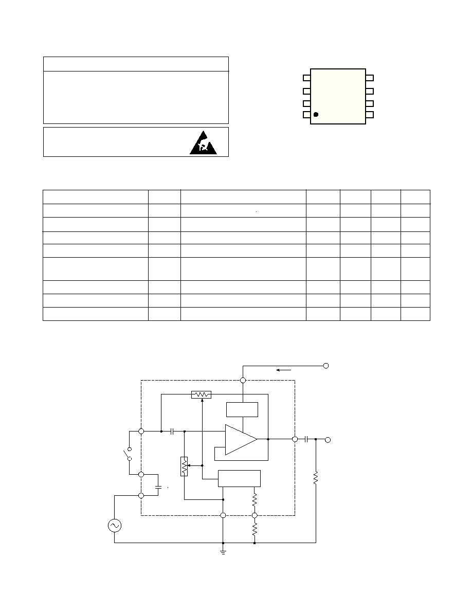
All parameters and switches remain as shown in Test Circuit unless otherwise stated in "Conditions" column
Notes: 1.
V
B
modulated with 1kHz
2.
F
C
= 1000 x 2
A
; A = (
I
LOSS
-
20
LOG
(V
OUT
/0.04))/12
V
OUT
R
CNT
100K
R
L
=10K
1.8K
V
B
A
CONTROL
8
5
3
4
7
1
+
_
1n0
1n0
VREG
=1.3VDC
1µ0
I
AMP
VI
N
1kHz
6
SW1
+
+
All resistors in ohms, all capacitors
in farads unless otherwise stated
Fig. 1 Test Circuit
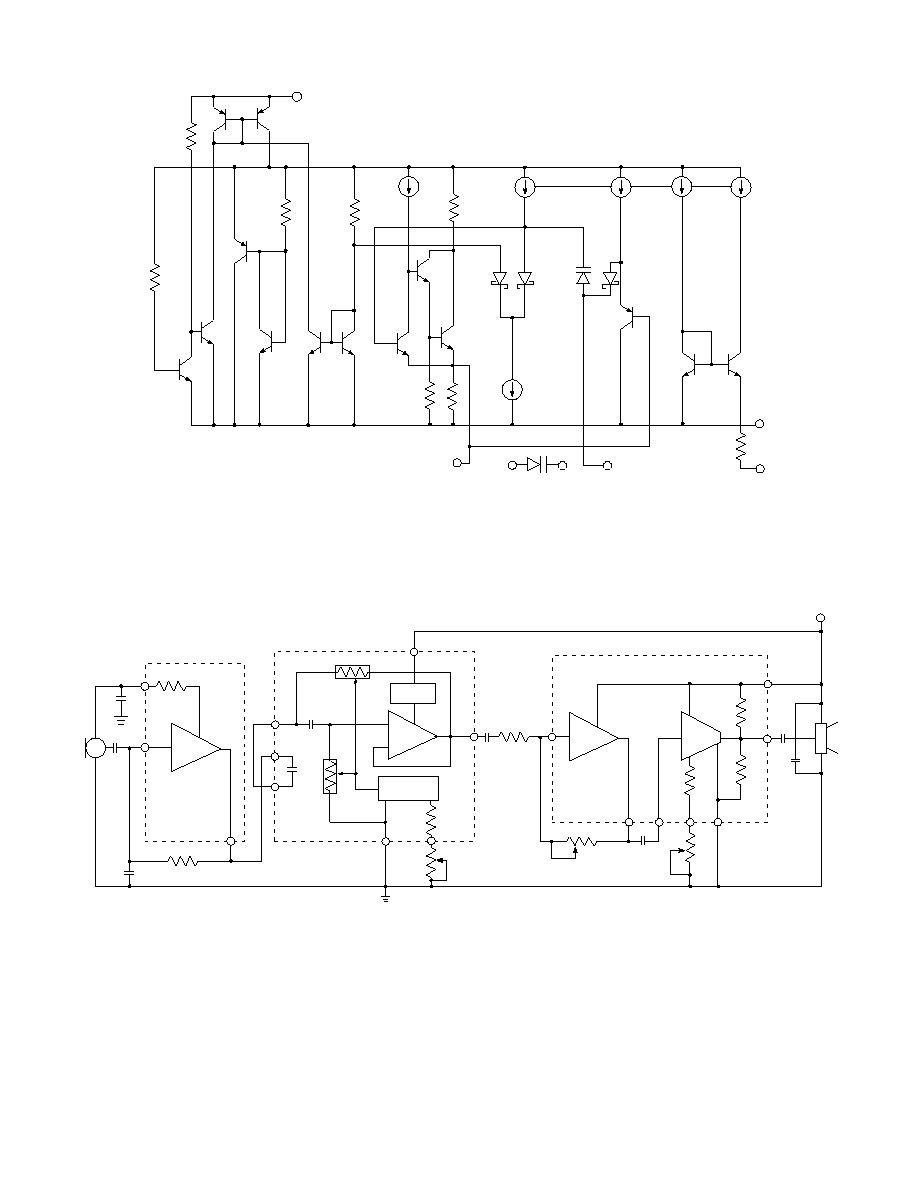
3
520 - 50 - 05
1.8K
1n
5
6
3
1
4
2
1n
7
8
All resistors in ohms, all capacitors in farads unless otherwise stated
Fig. 2 Functional Schematic
10K
EP
3075
1.3 VDC
0µ1
R
MIC
R
GT
100K
1µ0
GK504
2
1
3
0µ1
RCNT
100K
1k8
8
5
6
3
4
7
1
1n0
1n0
MIC
GH580
VREG
CONTROL
R
MPO
10K
7
R
VC
100K
33n
R
P1
33n
1µ0
10
9
8
6
5
4
- B
GK504
1/
2
- C
R
P2
- A
A
+
_
1n5
1/
2
+
+
All resistors in ohms, all capacitors in farads unless otherwise stated
Fig. 3 Typical Hearing Instrument Application
4
520 - 50 - 05
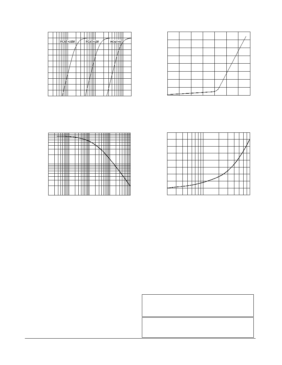
2
0
-2
-4
-6
-8
-10
-12
-14
-16
-18
-20
20
200
2k
20k
FREQUENCY (Hz)
THD (%)
10 20 30 40 50 60 70 80
INPUT (mV
RMS
)
RELATIVE OUTPUT (dB)
200 1k 8k
CORNER FREQUENCY (Hz)
215
210
205
200
195
190
185
180
175
170
CURRENT DRAIN (
µ
A)
1k
10k
100
10
100 1k 10k 100k
CONTROL RESISTANCE (
)
CORNER FREQUENCY (Hz)
16
14
12
10
8
6
4
2
0
Fig. 7 Current Drain vs Corner Frequency
Fig. 6 Corner Frequency vs Control Resistance
Fig. 4 Frequency Response at Various R
CNT
Values
Fig. 5 Total Harmonic Distortion vs Input Level
DOCUMENT IDENTIFICATION:
DATA SHEET
The product is in production. Gennum reserves the right to make
changes at any time to improve reliability, function or design, in
order to provide the best product possible.
Gennum Corporation assumes no responsibility for the use of any circuits described herein and makes no representations that they are free from patent infringement.
© Copyright November 1991 Gennum Corporation. All rights reserved. Printed in Canada.
REVISION NOTES:
Changes to standard packaging information
GENNUM CORPORATION
MAILING ADDRESS:
P.O. Box 489, Stn. A, Burlington, Ontario, Canada L7R 3Y3
Tel. +1 (905) 632-2996 Fax +1 (905) 632-2814
SHIPPING ADDRESS:
970 Fraser Drive, Burlington, Ontario, Canada L7L 5P5
GENNUM JAPAN CORPORATION
C-101, Miyamae Village, 2-10-42 Miyamae, Suginami-ku, Tokyo 168-0081,
Japan Tel. +81 (3) 3334-7700 Fax: +81 (3) 3247-8839