 | –≠–ª–µ–∫—Ç—Ä–æ–Ω–Ω—ã–π –∫–æ–º–ø–æ–Ω–µ–Ω—Ç: GK504 | –°–∫–∞—á–∞—Ç—å:  PDF PDF  ZIP ZIP |

A
V
MIC
R
MIC
A
IN
A
OUT
B
IN
GND
C
OUT
V
B
3
2
4
5
7
8
9
R
P1
B
C
6
1
10
B
OUT
R
MPO
C
IN
R
P2
FEATURES
∑
designed to drive Class D integrated receivers
∑
adjustable peak clipper
∑
low current drain
∑
low noise and distortion
∑
low external parts count
∑
two low noise preamplifiers
∑
transconductance output stage
∑
mid supply referenced output
∑
preamp A for Gain Trim or Telecoil
Low Current Preamplifier
with Output Limiting
DESCRIPTION
The GK504 is Gennum's proprietary low current preamplifier
designed to drive the Class D series receivers. It consists of
two independent single-ended, low noise inverting amplifiers,
a symmetrical peak clipping, mid-supply referenced,
transconductance output stage, and an on-chip microphone
decoupling resistor.
Blocks A and B typically have an open loop voltage gain of
53 dB, with the closed loop gain set by the ratio of the feedback
resistor to source impedance. It is recommended that the
maximum closed loop gain be 20 dB lower than the open loop
gain. All blocks of the device are internally bias compensated
preventing any DC current flow via external feedback resistors.
Without this compensation, audible scratchiness would be
present during changes in Volume Control settings. It is
acceptable to DC-couple blocks A and B of the device,
however the third stage must be AC coupled in order to
maintain DC bias requirements.
The major advantage of the GK504 over other preamplifiers is
the electronic MPO adjustment. Since conventional MPO is
not possible in the class D receivers, it is provided electronically.
The maximum output swing is easily set using an R
MPO
resistor.
The receiver output level is thus limited, preventing it from
exceeding the discomfort level.
Document No. 520 - 47 - 05
BLOCK DIAGRAM
STANDARD PACKAGING
∑ 10 pin MICROpac
∑ 10 pin PLID
Æ
∑ 10 pin SLT
∑ Chip ( 56 x 84 mils)
Au Bump
U.S. Patent No.07/354,327
GK504 - DATA SHEET
Revision Date; May 1998
GENNUM CORPORATION P.O. Box 489, Stn. A, Burlington, Ontario, Canada L7R 3Y3 tel. +1 (905) 632-2996
Web Site: www.gennum.com E-mail: hipinfo@gennum.com

2
520 - 47 - 05
PARAMETER
SYMBOL
CONDITIONS
MIN
TYP
MAX
UNITS
Supply Current
I
AMP
165
240
315
µ
A
Input Referred Noise
IRN
NFB 0.2 ≠ 10 kHz at 12 dB/oct
-
2
-
µ
V
RMS
Distortion
THD
-
<1.0
-
%
On-Chip Microphone Resistance
R
MIC
3
4
5
k
STAGES A and B
Input Bias Current
I
BIAS
R
F
=1M (Note 1)
-25
0
25
nA
Input Bias Voltage
V
BIAS
500
590
650
mV
Output Swing Lo
V
OL
R
F
=1M (Note 2)
200
280
590
mV
Max Output Current Capability
I
MAX
-15
-30
-45
µ
A
Open Loop Voltage Gain
A
VOL
46
53
-
dB
OUTPUT STAGE
Voltage Gain (Pin 8 to Pin 5)
A
V
V
IN
AC = -52 dBV, R
MPO
= 0
14
16
18
dB
Gain Loss (Pin 8 to Pin 5)
GAIN
V
IN
= -62 dBV, R
MPO
= 50k,Note 3
-
0
2.5
dB
Maximum Output Level
MPO
V
IN
AC = -22 dBV, R
MPO
= 0
-14.5
-12.5
-10.5
dBV
MPO Range
MPO
V
IN
AC = -22 dBV,R
MPO
= (0 to 10k)
12
14
16
dB
Output Impedance
Z
OUT
19
24
29
K
Parameter
Value / Units
Supply Voltage
5 VDC
Power Dissipation
25 mW
Operating Temperature
-10
∞
C to + 40
∞
C
Storage Temperature
-20
∞
C to + 70
∞
C
ABSOLUTE MAXIMUM RATINGS
CAUTION
CLASS 1 ESD SENSITIVITY
5
10
1
6
R
MPO
A
OUT
GND
C
IN
B
OUT
B
IN
C
OUT
V
B
V
MIC
A
IN
PIN CONNECTIONS
ELECTRICAL CHARACTERISTICS
Positive Current corresponds to current INTO the pin, Negative Current corresponds to current OUT of the pin, Conditions: Frequency = 1 kHz,
Temperature 25
o
C.
V
P
- Pin voltage measured with conditions as shown in Test Circuit.
All parameters and conditions remain as shown in Test Circuit unless otherwise specified in Conditions column.
NOTES: 1.
I
BIAS
= (Vp(1,9 ) ≠ Vp(1,9 )
[RF=1M]
)/1M
2.
V
OL
= V
BIAS
-Vp(1,9)
[VIN DC=+1
µ
A,RF=1M,IL=+15
µ
A]
3.
GAIN = (V
OUT
/ V
IN
[VIN =-62dBV, RMPO=0]
)- (V
OUT
/ V
IN
[VIN =-62dBV, RMPO=50k]

3
520 - 47 - 05
A
B
=1.3 VDC
V
B
OUT
V
4
5
8
R
P1
6
9
10
1
3
R
MIC
2
R
F
=0
7
IN
V
DC
0
µ
1
I
AMP
C
R
P2
I
BIAS
I
BIAS
V
IN
DC
V
IN
AC=
0V
RMS
1kHz
R
L
50k
R
MPO
=10k
I
L
=0
I
L
=0
R
F
=0
1
µ
0
All resistors in ohms, all capacitors in
µ
F, unless otherwise stated.
Fig. 1 Test Circuit
All resistors in ohms, all capacitors in
µ
F, unless otherwise stated.
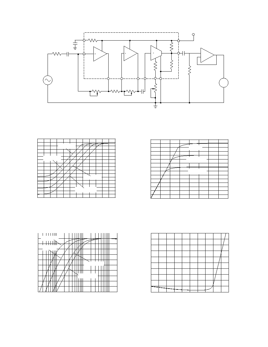
Fig. 2 Functional Schematic
BASE CURRENT
COMPENSATION
3
R
MIC
2
10
1
9
2.5k
33k
7
8
48k
6
5
48k
4

4
520 - 47 - 05
A
=1.3 VDC
V
B
5
R
P1
6
R
MPO
10
1
10k
3
R
MIC
2
1
µ
0
4
100k
0
µ
47
R
VC
9
C
B
100k
R
GT
R
P2
7
8
0
µ
22
MIC
-
+
33n
10k
33n
Class D
Integrated Receiver
1
µ
0
A
=1.3 VDC
V
B
Class D
Integrated Receiver
5
R
P1
6
R
MPO
1
µ
0
10
1
10k
3
R
MIC
2
1
µ
0
4
100k
C
IN
0
µ
22
R
VC
9
B
100k
R
GT
R
P2
7
8
MIC
33n
10k
33n
C
Fig. 3 Typical Hearing Instrument Application
All resistors in ohms, all capacitors in
µ
F, unless otherwise stated.
Fig. 4 Typical Hearing Instrument Application
All resistors in ohms, all capacitors in
µ
F, unless otherwise stated.
5
520 - 47 - 05
A
=1.3 V
DC
V
B
5
R
P1
6
R
MPO
10
1
10k
3
R
MIC
2
1
µ
0
4
100k
R
VC
9
C
B
100k
R
GT
R
P2
7
8
0
µ
22
0
µ
1
=0
0
µ
1
CS
+
-
BUFFER
AC SOURCE
50
R
MIC
3k92
AC
VOLTMETER
R
L
50k
2
0
-2
-4
-6
-8
-10
-12
-14
-16
-18
-20
-90 -86 -82 -78 -74 -70
10
9
8
7
6
5
4
3
2
1
0
INPUT (dBV)
20
200
2K 20K
FREQUENCY (Hz)
Fig. 8 Frequency Response for Various C
IN
Values
C
IN
= 0.22
µ
C
IN
= 0.033
µ
C
IN
= 0.1
µ
C
IN
= 0.047
µ
Fig. 9 Distortion vs Input Level (R
GT
= R
VC
= 100k)
RELATIVE OUTPUT (dB)
THD (%)
All resistors in ohms, all capacitors in
µ
F, unless otherwise stated.
This circuit as shown was used to generate the following graphs unless
otherwise stated.
Fig. 5 Characterization Circuit
OUTPUT (dBV)
Fig. 7 MPO for Various R
MPO
Values
R
VC
= 100k
R
VC
= 33k
R
VC
= 10k
R
VC
= 3.3k
-140 -120 -100 -80 -60 -40 -20
-5
-15
-25
-35
-45
-55
-65
-75
-85
INPUT (dBV)
OUTPUT (dBV)
-10
-14
-18
-22
-26
-30
-34
-38
-100 -80 -60 -40 -20
INPUT (dBV)
Fig. 6 I/O for Various R
VC
Values
R
MPO
= 10k
R
MPO
= 3.3k
R
MPO
= 0

6
520 - 47 - 05
55
50
45
40
35
0 10 100 1k 10k 100k
Fig. 12 Maximum Output vs R
MPO
(as in Fig. 1, V
IN
AC= -15dBV)
MAXIMUM OUTPUT (dBV)
R
MPO
(
)
Fig. 13 Preamplifiers A and B
Open Loop Voltage Gain
FREQUENCY (Hz)
-10
-14
-18
-22
-26
-30
-34
-38
-42
GAIN (dB)
10 100 1k 10k 100k
RELATIVE SUPPLY CURRENT (
µ
A)
Fig. 10 Change in Supply Current vs R
MPO
INPUT (dBV)
-50 -40 -30 -20 -10 0
-12
-16
-20
-24
-28
-32
-36
OUTPUT (dBV)
R
MPO
(
)
10
-10
-30
-50
-70
-90
-110
-130
1 10 100 1k 10k 100k
Fig. 11 I/O for Amplifier C
(as in Fig. 1)
1.3V
PREAMP
10µ
10µ
VAC
2.2k
1M
1M
VOUT
DOCUMENT IDENTIFICATION:
DATA SHEET
The product is in production. Gennum reserves the right to make
changes at any time to improve reliability, function or design, in
order to provide the best product possible.
Gennum Corporation assumes no responsibility for the use of any circuits described herein and makes no representations that they are free from patent infringement.
© Copyright July 1990 Gennum Corporation. All rights reserved. Printed in Canada.
REVISION NOTES:
Updated to Data sheet