 | –≠–ª–µ–∫—Ç—Ä–æ–Ω–Ω—ã–π –∫–æ–º–ø–æ–Ω–µ–Ω—Ç: GL504 | –°–∫–∞—á–∞—Ç—å:  PDF PDF  ZIP ZIP |

A
R
MIC
R
MIC
A
IN
A
OUT
B
IN
MPO
GND
B
OUT
V
B
R
PULL
R
CLIP
6
5
7
8
1
2
3
4
B
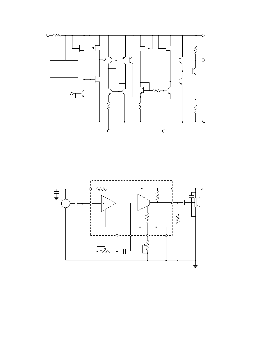
BLOCK DIAGRAM
DESCRIPTION
The GL504 is a low current preamplifier designed to drive
the class D series of integrated receivers. This preamp has a
built-in symmetrical peak clipping output limiter, 46 dB of
adjustable gain, and requires few external components.
Composed of two stages, an inverting preamp with gain of
28 dB, and a transconductance block with gain of 18 dB, the
GL504 is easily configured for mid-supply reference as
required by the class D receivers.
The two stages of the GL504 must be AC coupled in order to
maintain the DC bias conditions of each stage. Also, a 48
k
resistor, between the output and ground, is used to keep
the receivers at mid-supply reference. The minimal total parts
count, excluding an MPO variable resistor, requires 3
capacitors, a 100 k
volume control and the 48 k
bias
resistor at the output.
The GL504 is capable of providing a flat frequency response
with very little distortion.
FEATURES
∑
designed to drive class D integrated receivers
∑
MPO range externally adjustable
∑
150
µ
A typical current drain
∑
46 dB of adjustable gain
∑
low external parts count
∑ 8 Pin MICROpac
∑ 8 Pin PLID
Æ
∑ 8 Pin SLT
∑ Chip (56 x 56 mils)
Au Bump
STANDARD PACKAGING
Document No. 510 - 99 - 06
GL504 - DATA SHEET
Low Current Preamplifier
with Output Limiting
U.S. Patent No. 07/354,327
Revision Date: May 1998
GENNUM CORPORATION P.O. Box 489, Stn. A, Burlington, Ontario, Canada L7R 3Y3 tel. +1 (905) 632-2996
Web Site: www.gennum.com E-mail: hipinfo@gennum.com

2
510 - 99 - 06
PARAMETER
VALUE / UNITS
Supply Voltage
5 V
Operating Temperature
-10
∞
C to +40
∞
C
Storage Temperature
-20
∞
C to +70
∞
C
ABSOLUTE MAXIMUM RATINGS
Fig. 1 Test Circuit
PIN CONNECTION
1
4
5
8
A
OUT
B
IN
MPO
GND
A
IN
R
MIC
B
OUT
All resistors in ohms, all capacitors in
µ
F, unless otherwise stated.
V
B
CAUTION
Class 1 ESD Sensitivity
PARAMETER SYMBOL
CONDITIONS
MIN
TYP
MAX
UNITS
Amplifier Current
I
AMP
R
MPO
= 0
75
150
225
µ
A
Microphone Resistance
R
MIC
3.0
4.0
5.3
k
Input Referred Noise
IRN
NFB 0.2 to 10kHz at 12 dB/oct
-
2
-
µ
V
RMS
Gain
A
V
V
IN
= -80 dBV
44.5
46.5
48.5
dB
MPO Level
MPO
V
IN
= -50 dBV
-16
-14
-12
dBV
R
MPO
= 0
Change in MPO
MPO
V
IN
= -50 dBV
10
12
14
dB
R
MPO
= 10 k
Preamp A input Bias Current
I
BIAS A
-25
0
+25
nA
Pull-up Resistance
R
PULL
40
48
58
k
Gain Loss
GAIN
R4 = 10 k, V
IN
= -70 dBV,
-
0
2.5
dB
R
MPO
= 50 k
ELECTRICAL CHARACTERISTICS
(refer to test circuit) Supply Voltage = 1.3 V, Test Frequency 1kHz
A
B
47k
=1.3 VDC
V
B
OUT
V
0
µ
1
7
R
PULL
R
CLIP
1
R
MPO
2
3
4
0
µ
1
R4
6
R
MIC
5
3k9
10
1k
IN
V
0
µ
22
IN
V
1+40 dB
8
A
100k
I
AMP
3
510 - 99 - 06
Fig. 2 Functional Schematic
Fig. 3 Typical Application Circuit
All resistors in ohms, all capacitors in
µ
F, unless otherwise stated.
All resistors in ohms, all capacitors in
µ
F,
unless otherwise stated.
6
33k
2
7
8
4
1
BASE CURRENT
COMPENSATION
5
3
R
MIC
2k5
R
PULL
A
=1.3 VDC
V
B
CLASS D
INTEGRATED
RECEIVER
33n
7
R
PULL
R
CLIP
1
R
MPO
10k
3
4
22n
5
R
6
1
µ
0
8
100k
0
µ
1
48k
B
R
VC
2
1
µ
0
MIC
MIC

4
510 - 99 - 06
OUTPUT (
d
BV)
R
MPO
= 0
R
MPO
= 3k3
R
MPO
= 10k
INPUT (dBV)
Fig. 5 I/O for Various MPO Values
OUTPUT (
d
BV)
R
VC
= 3k3
R
VC
= 100k
R
VC
= 33k
R
VC
= 10k
-140 -120 -100 -80 -60
-40 -20
INPUT (dBV)
Fig. 4 I/O Curves at Various R
VC
Settings
THD (%)
INPUT (dBV)
Fig. 7 Distortion vs Input Level (R
VC
=100k
)
FREQUENCY (Hz)
C
S
= 0
µ
22
C
S
= 0
µ
1
C
S
= 0
µ
047
C
S
= 0
µ
033
20 200 2k 20k
Fig. 6 Frequency Response for Various C
S
Values
RELATIVE OUTPUT (
d
B)
RELATIVE AMPLIFIER CURRENT (
µ
A)
R
MPO
(k
)
Fig. 8 Quiescent Current vs MPO Resistance
-10
-20
-30
-40
-50
-60
-70
-80
-90
4
0
-4
-8
-12
-16
-20
0
-10
-20
-30
-40
-50
-60
-70
-80
-90
-10
-15
-20
-25
-30
-35
-40
-45
-50
-100
-80 -60
-40
-20
10
9
8
7
6
5
4
3
2
1
0
-90 -86 -82 -78 -74 -70 -66 -62 -58
0 5 10 15 20 25 30

5
510 - 99 - 06
GAIN (dB)
55
50
45
40
35
10 100 1k 10k 100k
FREQUENCY (Hz)
Fig. 10 Preamplifier A Open Loop Voltage Gain
Fig. 9 Output vs MPO Resistance
No Load
50k Load
R
MPO
(
)
OUTPUT (
d
BV)
-10
-14
-18
-22
-26
-30
-34
-38
-42
-46
-50
0 10 100 1k 10k 100k
DOCUMENT IDENTIFICATION:
DATA SHEET
The product is in production. Gennum reserves the right to make
changes at any time to improve reliability, function or design, in
order to provide the best product possible.
Gennum Corporation assumes no responsibility for the use of any circuits described herein and makes no representations that they are free from patent infringement.
© Copyright July 1990 Gennum Corporation. All rights reserved. Printed in Canada.
REVISION NOTES:
Updated to Data sheet