
GENNUM CORPORATION P.O. Box 489, Stn. A, Burlington, Ontario, Canada L7R 3Y3
Tel. +1 (905) 632-2996 Fax. +1 (905) 632-5946 E-mail: info@gennum.com
www.gennum.com
Revision Date: March 2000
Document No. 522 - 40 - 02
DATA SHEET
GO1
5
1
5
FEATURES
∑ generates 1.485GHz or 1.485/1.001GHz signal for
HD-LINXTM ICs
∑ low current consumption
∑ 50
output impedance
∑ operates from a single 5V supply
∑ 8 pin tape on reel
APPLICATIONS
VCO for the following HD-LINXTM ICs: GS1515, GS1522,
GS1540, GS1545.
DESCRIPTION
The GO1515 is a self contained, miniature Voltage
Controlled Oscillator (VCO) that is used in conjunction with
Gennum's HD-LINXTM ICs. It produces a clean 1.485GHz
reference clock signal for such devices as the GS1515
HDTV Reclocker and other HD-LINXTM devices. The control
voltage range is from 3.10 volts to 4.65 volts and is derived
from the on-chip PLLs. The GO1515 frequency can be
pulled approximately 16MHz for every one volt of control.
The output level is approximately 1.0dBm with low spurious
and noise content. It is designed to drive 50
strip lines.
The GO1515 VCO is used with the following HD-LINXTM ICs;
GS1515, GS1522, GS1540, GS1545 and is ordered as a
separate item. The VCO requires a single 5V supply and
draws a maximum of 15mA of current. It is packaged in a
miniature 8-pin proprietary surface mount package and
operates over the normal commercial temperature range of
0∞C to +70∞C.
BLOCK DIAGRAM
ORDERING INFORMATION
PART NUMBER
PACKAGE
TEMPERATURE
GO1515 - CTA
8 pin tape on reel
0∞C to 70∞C
OSCILLATOR CIRCUIT
1000pF
47pF
STRIPLINE
STRIPLINE
3.3pF
2pF
V
CTR
V
CC
OUT
GND
HD-LINX
TM
GO1515
Voltage Controlled Oscillator
522 - 40 - 02
2
G
O
1
515
PIN CONNECTIONS
ELECTRICAL CHARACTERISTICS
V
S
= 5.0V ±0.25V, Temperature = 0∞C to 70∞C unless otherwise specified.
PARAMETER
SYMBOL
CONDITIONS
MIN
TYP
MAX
UNITS
Supply Voltage
V
CC
4.75
5.0
5.25
V
Supply Current
S
-
-
15
mA
Control Voltage Range
V
CTR
+3.1
-
+4.65
V
Control Voltage Sensitivity
df/dV
11
16
21
MHz/V
Operating Frequency
Range
VCO
1483.5
-
1485.5
MHz
Output Signal Level
V
OUT
-2
1
+4
dBm
Signal to Noise Ratio
S/N
Signal Level: 1kHz ±8kHz
Deviation = 0.3~3.0kHz
40
-
-
dB
Carrier to Noise Ratio
C/N
25kHz Separation, 1kHz Bandwidth
74
-
-
dBc
Pushing Figure
V
S
= 5.0V ±0.25V, ref: V
S
= 5.0V
-
±500
-
kHz
Pulling Figure
VSWR = 2.0 for all phase, ref: 50
-
±1000
-
kHz
Temperature Stability
T
COEF
0∞C to 70∞C, ref. = 25∞C
-
-
±3
MHz
Spurious Response
-
-
-10
dBc
Output Impedance
Z
O
-
50
-
PIN DESCRIPTIONS
NUMBER
SYMBOL
TYPE
DESCRIPTION
2, 4, 6, 8
GND
-
Most negative power supply connections.
1
V
CTR
I
Control voltage for the VCO.
3
V
CC
-
Most positive power supply connection.
5
O/P
O
VCO signal output.
7
NC
-
No connection.
GO
1515
NC
GND
O/P
GND
GND
GND
V
CC
V
CTR
7
6
5
8
4
1
3
2
NOTE: Pin numbers are arbitrary.
There are no pin markings on the device itself
TOP VIEW

522 - 40 - 02
3
GO1
5
1
5
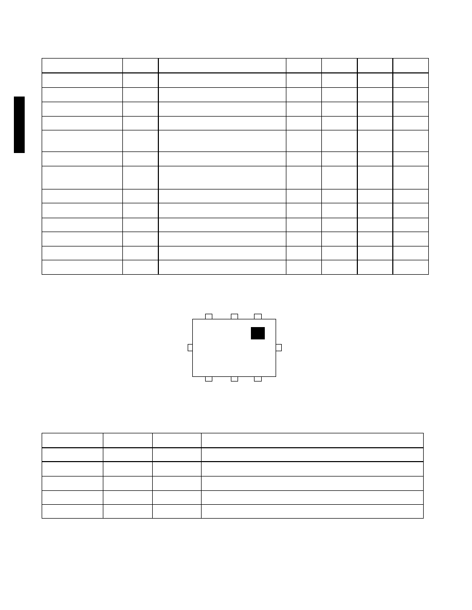
Fig. 1 Footprint of the GO1515
DIMENSIONS
SOLDERING RECOMMENDATIONS
Reflow Conditions
The device will meet the data sheet specifications after
completing the reflow process according to the profile
shown in Figure 3. Do not reflow the device more than
twice.
Endurance To Warp
When the device is soldered on a printed circuit board
(dimension: 100mm x 100mm; thickness: 1.6mm) and the
PCB is warped as shown in Figure 2, the device will not be
cracked or damaged.
Fig. 3 PCB Warp
Soldering Conditions
Recommended soldering conditions are as follows:
Reflow Soldering
Preheating
150±10∞C, 60 to 120 sec.
Soldering
Peak 230±5∞C
Over 200∞C within 30 sec.
Soldering Flux
Do not use cleaning type flux. Washing the devices after
using cleaning type flux may damage inner parts and affect
performance.
Solder Type
Use solder H60, H63 (in JIS Z 3282) or an equivalent type.
This also applies to solder paste.
OUT
NC
GND
V
CC
V
CTR
GND
65
55
40
40
55
65
45
GND
GND
GO1515
TOP VIEW
All dimensions are in mils
1 mil = 1/1000 inch
GO1515
TOP VIEW
2.0
±0.3
4.2
±0.3
6.0
MAX
1.6±0.5
4.7±0.3
6.3±0.3
7.8 MAX
All dimensions in millimetres.
NC
GND
OUT
V
CC
V
CTR
GND
GND
GND
2.0 MAX
VCO
PCB
MAX 2mm

522 - 40 - 02
4
GENNUM CORPORATION
MAILING ADDRESS:
P.O. Box 489, Stn. A, Burlington, Ontario, Canada L7R 3Y3
Tel. +1 (905) 632-2996 Fax. +1 (905) 632-5946
SHIPPING ADDRESS:
970 Fraser Drive, Burlington, Ontario, Canada L7L 5P5
GENNUM JAPAN CORPORATION
C-101, Miyamae Village, 2-10-42 Miyamae, Suginami-ku
Tokyo 168-0081, Japan
Tel. +81 (03) 3334-7700 Fax. +81 (03) 3247-8839
GENNUM UK LIMITED
25 Long Garden Walk, Farnham, Surrey, England GU9 7HX
Tel. +44 (0)1252 747 000 Fax +44 (0)1252 726 523
Gennum Corporation assumes no responsibility for the use of any circuits described herein and makes no representations that they are free from patent infringement.
© Copyright June 1999 Gennum Corporation. All rights reserved. Printed in Canada.
G
O
1
515
Fig. 3 Reflow Profile
HANDLING RECOMMENDATIONS
Cleaning
Do not wash the devices.
Storage
Store the devices out of direct sunlight, at a stable
temperature and humidity. Avoid extreme temperatures,
high humidity and wide temperature fluctuations.
Condensation on the devices may result in reduced quality
and lowered solderability.
Use within 6 months after delivery. If the devices are stored
for more than one year, solderability may be degraded.
Avoid dust, sea breezes and corrosive gases (Cl
2
, NH
3
,
SO
2
, NO
X
, etc.).
60 to 120 sec
60 sec
30 sec
230 ± 5
200
160
140
TIME (sec.)
TEMPERA
TURE (∞C)
REVISION NOTES:
Added Soldering and Handling sections and figures.
For latest product information, visit www.gennum.com.
DOCUMENT IDENTIFICATION
DATA SHEET
The product is in production. Gennum reserves the right to make
changes at any time to improve reliability, function or design, in order to
provide the best product possible.
CAUTION
ELECTROSTATIC
SENSITIVE DEVICES
DO NOT OPEN PACKAGES OR HANDLE
EXCEPT AT A STATIC-FREE WORKSTATION