 | –≠–ª–µ–∫—Ç—Ä–æ–Ω–Ω—ã–π –∫–æ–º–ø–æ–Ω–µ–Ω—Ç: GP509 | –°–∫–∞—á–∞—Ç—å:  PDF PDF  ZIP ZIP |
GENNUM CORPORATION P.O. Box 489, Stn A, Burlington, Ontario, Canada L7R 3Y3 tel. (905) 632-2996 fax: (905) 632-2055
Japan Branch: A-302, M i yamae Vi l l age, 2≠10≠42 M i yamae, Suginami≠ku, Tokyo 168, Japan tel. (03) 3247-8838 fax (03) 3247-8839
Class A Amplifier with
2 Independent Gain Blocks
GP509 DATA SHEET
Document No. 510 - 71 - 04
FEATURES
∑
low amplifier current (typical 105
µ
A)
∑
low noise and distortion
∑
1.0 to 5 VDC operating range
∑
independent preamplifier
∑
Class A output stage
∑
variable transducer current
∑
4.0 k
microphone decoupling resistor, on-chip
DESCRIPTION
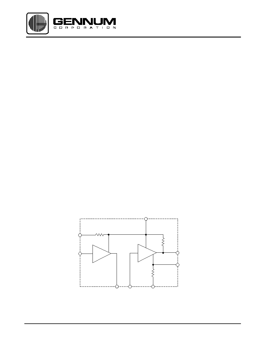
The GP509 is a Class A amplifier utilizing Gennum's proprietary
low voltage JFET technology. It consists of a single-
ended, low noise inverting gain block, a Class A output
stage, and an on-chip microphone decoupling resistor.
Block A typically has an open loop voltage gain of 56 dB,
with the closed loop gain set by the ratio of the feedback
resistor to the source impedance. It is recommended that
the maximum closed loop gain be 20 dB lower than the
open loop gain. All blocks of the device are internally bias
compensated, preventing any DC current flow via external
feedback resistors. Without this compensation, audible
scratchiness would be present during changes in volume
control settings.
The output stage of the GP509 is a Class A current drive.
It has a fixed reference voltage of typically 30 mV at pin 7
of the device. The current that flows in the transducer is the
ratio of the 30 mV reference voltage and the on-chip emitter
resistor (R
E
). To increase the bias current in the transducer,
simply place an external R
E
resistor from pin 7 to ground,
thereby decreasing the equivalent emitter resistance and
increasing the current.
STANDARD PACKAGING
∑ 8 pin MICROpac
∑ 8 pin PLID
Æ
∑ 8 pin SLT
∑ Chip (61 x 55 mils)
BLOCK DIAGRAM
-
A
-
B
B IN
R
B OUT
V
E
B
GND
A OUT
A IN
V
MIC
1
2
4
3
R
MIC
8
7
5
R
E
21k
6
Revision Date: January 1996

2
510 - 71 - 04
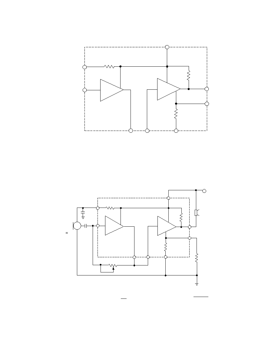
1.3 VDC
R =27.5
E
1.0
5
7
8
2
- B
- A
R
E
21k
6
R
L
= 1k
R
MIC
4
3
1
R =100k
FA
1 kHz
R
S
R
B
= 4.7
V
IN
S1
a
b
3k3
1.0
C
S
V
OUT
1
4
5
8
V
MIC
GND
A IN
A OUT
B IN
R
E
B OUT
V
B
PIN CONNECTION
ABSOLUTE MAXIMUM RATINGS
PARAMETER
VALUE / UNITS
Supply Voltage
5V DC
Power Dissipation
25 mW
Operating Temperature
-10
o
to + 40
o
C
Storage Temperature
-20
o
to + 70
o
C
CAUTION
CLASS 1 ESD SENSITIVITY
PARAMETER
SYMBOL CONDITIONS
MIN
TYP
MAX UNITS
Amplifier Current
I
AMP
55
105
150
µ
A
Transducer Current
I
TRANS
R
E
=
225
300
375
µ
A
Maximum Transducer Current
I
TRANS(MAX)
R
E
= 0
2
-
-
mA
Voltage Gain
A
V
S1 = b V
OUT
= 500 mV
RMS
58 61
64
dB
Harmonic Distortion
THD
S1 = b V
OUT
= 500 mV
RMS
-
1
4
%
Input Referred Noise
IRN
NFB 0.2 to 10 kHz at 12dB/Oct
-
1
2
µ
V
RMS
Stable with Battery Resistance
Resistance (R
B
) to:
Stability
R
B
= 22
-
- 22
Input Bias Current
I
BIAS
R
FA
= 1M
-50
0
50
nA
Microphone Resistance
R
MIC
3
4
5
k
Emitter Bias Voltage (Pin 7)
VRE
-
30
-
mV
On Chip Emitter Resistor
RE
-
100 -
A Output Current Capability
(Pin 1)
I
OUT
-
30
-
µ
A
Note: All parameters and switches as shown in Test Circuit unless otherwise stated in CONDITIONS column
ELECTRICAL CHARACTERISTICS
Supply Voltage = +1.3 VDC, Frequency = 1 kHz, Temperature = 25
o
C
All external resistors in ohms &
±
1% tol., all capacitors in farads &
±
10% tol. unless otherwise stated
Fig. 1 Test Circuit
3
510 - 71 - 04
-
A
-
B
B IN
R
B OUT
V
E
B
GND
A OUT
A IN
V
MIC
1
2
4
3
R
MIC
8
7
5
R
E
21k
6
10
R
S
10
A = 20 Log
R
VC
B = 20 Log R
LAC
// 21K
Gain of Stage
Gain of Stage
Fig. 3 Typical Hearing Aid Circuit
R
E
// 82
All resistors in ohms, all capacitors in farads unless otherwise stated.
Fig. 2 Functional Schematic
R
MIC
6
ED1913
R
LAC
2
V =1.3VDC
1
4
3
5
R
E
82
21k
7
-
A
1.0
B
C
S
0.22
-
B
100k
R
VC
R
s
3k9
8
4
510 - 71 - 04
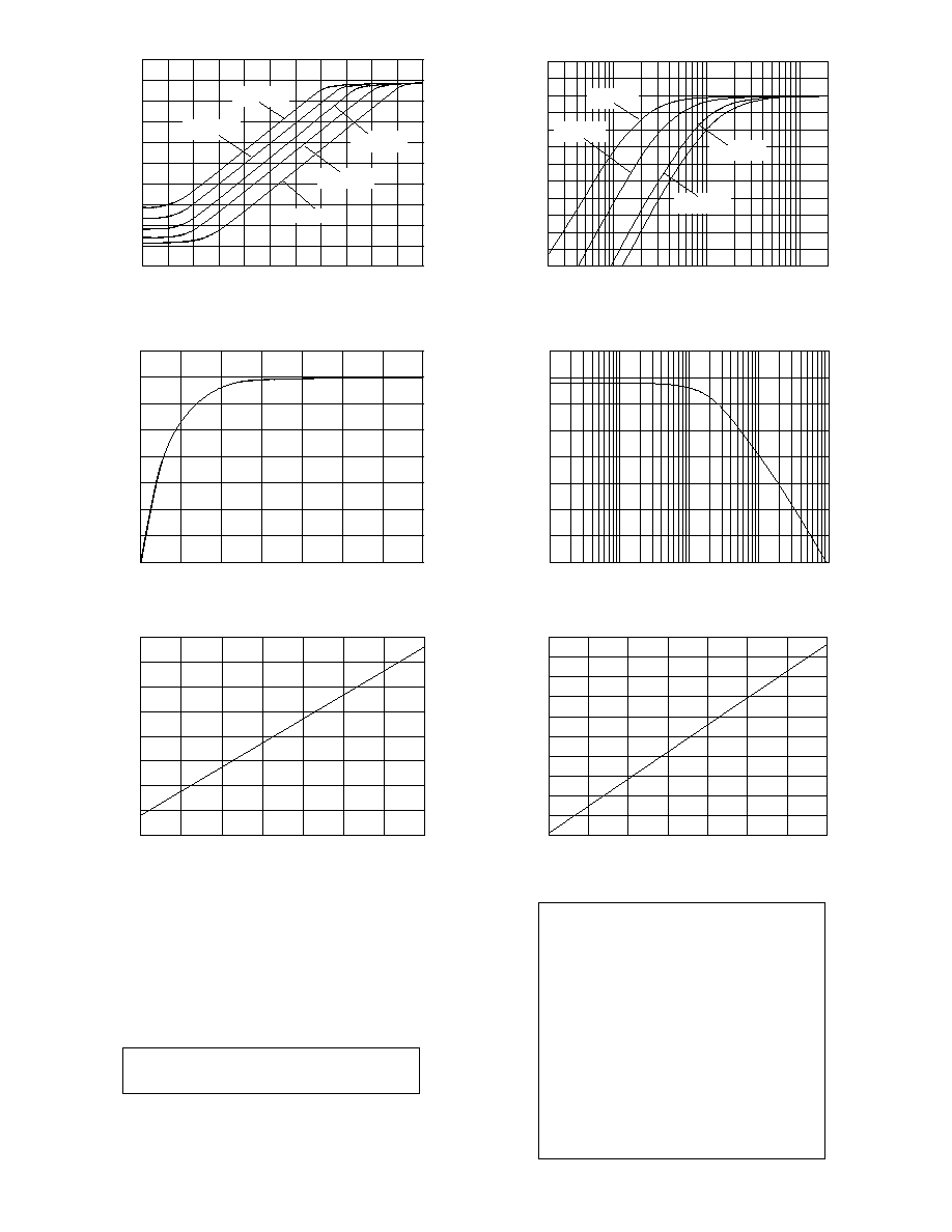
Fig. 8 Transducer Current vs Temperature
Fig. 9 Amplifier Current vs Temperature
-20 -10 0 10 20 30 40 50
TEMPERATURE (
O
C)
15
10
5
0
-5
-10
-15
-20
-25
RELATIVE TRANSDUCER CURRENT (
µ
A)
20
15
10
5
0
-5
-10
-15
-20
-25
-30
RELATIVE AMPLIFIER CURRENT (
µ
A)
-20 -10 0 10 20 30 40 50
TEMPERATURE (
O
C)
10 100 1K 10K 100K
FREQUENCY (Hz)
Fig.7 Preamplifier Open Loop Frequency Response
DOCUMENT
IDENTIFICATION
PRODUCT PROPOSAL
This data has been compiled for market investigation purposes
only, and does not constitute an offer for sale.
ADVANCE INFORMATION NOTE
This product is in development phase and specifications are
subject to change without notice. Gennum reserves the right to
remove the product at any time. Listing the product does not
constitute an offer for sale.
PRELIMINARY DATA SHEET
The product is in a development phase and specifications are
subject to change without notice.
DATA SHEET
The product is in production. Gennum reserves the right to make
changes at any time to improve reliability, function or design, in
order to provide the best product possible.
Gennum Corporation assumes no responsibility for the use of any circuits described
herein and makes no representations that they are free from patent infringement.
© Copyright 1989 Gennum Corporation. All rights reserved. Printed in Canada.
REVISION NOTES
Au bump removed
20 200 2k 20k
FREQUENCY (Hz)
C
S
= 0.22
µ
C
S
= 0.1
µ
C
S
= 0.047
µ
C
S
= 0.033
µ
4
2
0
-2
-4
-6
-8
-10
-12
-14
-16
-18
-20
OUTPUT (dBV)
Fig. 5 Closed Loop Frequency Response
for Various C
S
Values
60
55
50
45
40
35
30
25
20
GAIN (
d
B)
10
0
-10
-20
-30
-40
-50
-60
-70
-80
-90
OUTPUT (dBV)
INPUT (dBV)
R
VC
= 100k
R
VC
= 47k
R
VC
= 22k
R
VC
= 10k
-130 -120 -110 -100 -90 -80 -70 -60 -50 -40 -30 -20
Fig.4 I/O Characteristics for Various Gain Settings
Fig.6 Gain vs Supply Voltage
0.7 0.8 0.9 1.0 1.1 1.2 1.3 1.4
SUPPLY VOLTAGE (V)
5
0
-5
-10
-15
-20
-25
-30
-35
RELATIVE GAIN (
d
B)
R
VC
= 3.3k