GENNUM CORPORATION P.O. Box 489, Stn. A, Burlington, Ontario, Canada L7R 3Y3
Tel. +1 (905) 632-2996 Fax. +1 (905) 632-5946 E-mail: info@gennum.com
www.gennum.com
Revision Date: January 2000
Document No. 522 - 23 - 01
PRELIMINARY DATA SHEET
G
S
1
515
FEATURES
∑ SMPTE 292M compliant
∑ fully automatic adjustment free reclocker for HDTV
signals
∑ 1.485Gb/s and 1.485/1.001Gb/s operation
∑ dual 75
co-axial cable driver outputs
∑ reclocker bypass mode
∑ seamless input Interface to the GS1504 HD adaptive
equalizer
∑ low power
∑ lock detect
∑ +5V or -5V power supply operation
∑ 44 pin MQFP
APPLICATIONS
SMPTE 292M Serial Digital Routers; SMPTE 292M Serial
Digital Distribution Amplifiers.
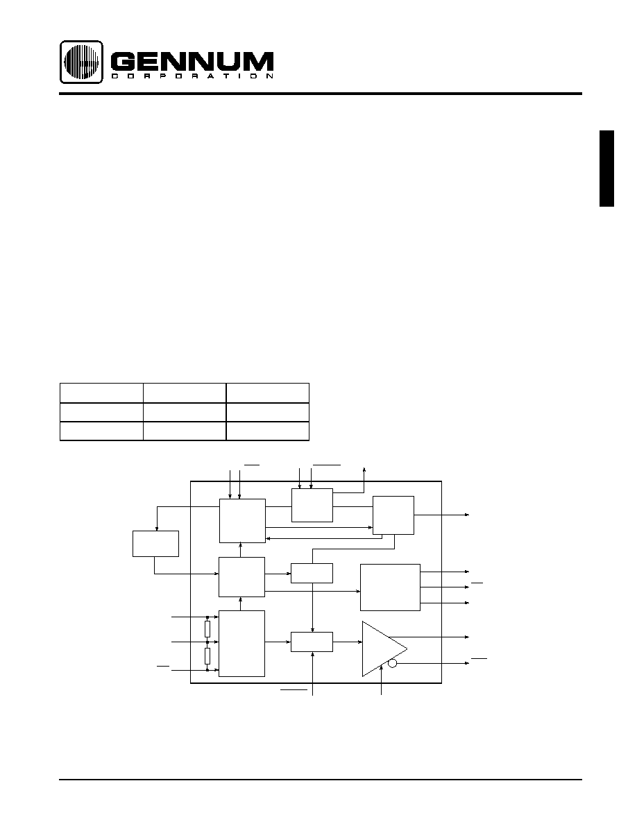
DESCRIPTION
The GS1515 HDTV Serial Digital Reclocker is designed to
automatically recover the embedded clock signal and re-
time the data from a SMPTE 292M compliant digital video
signal.
An internal low pass filter removes the high frequency jitter
components from the bit-serial stream. 100
differential
input termination is on-chip for seamless matching to 50
transmission lines. A dual SMPTE 292M compliant output
Cable Driver is also included on-chip. The GS1515 uses the
GO1515 external VCO connected to the internal PLL
circuitry in order to achieve ultra low noise PLL
performance.
Two diagnostic features are included in the GS1515 for
robust system design. The Input Jitter Indicator (IJI)
indicates excessive input jitter before the Serial Digital
outputs are muted and the Jitter Demodulator Function
(DM) helps to debug systems and locate the source of jitter.
The GS1515 is packaged in a 44 pin MQFP package and
requires a single 5V power supply. The GS1515 typically
draws 100mA of current.
BLOCK DIAGRAM
ORDERING INFORMATION
PART NUMBER
PACKAGE
TEMPERATURE
GS1515-CQM
44 pin MQFP
0∞C to 70∞C
GS1515-CTM
44 pin MQFP Tape
0∞C to 70∞C
GO1515
VCO
CHARGE
PUMP
PHASE
LOCK
PHASE
DETECTOR
MUTE
JITTER
DEMODULATOR
INPUT
BUFFER
LFA
VCO
LFS
LFS
PLCAP
PLCAP
IJI
LOGIC
PLL_LOCK
DM
DM
SDO
SDO
DFT_V
EE
R
SET
BYPASS
CABLE
DRIVER
BYPASS
50
50
DDI
DDI_V
TT
DDI
PATENT PENDING
HD-LINX
TM
GS1515
HDTV Serial Digital Reclocker

522 - 23 - 01
2
G
S
151
5
ABSOLUTE MAXIMUM RATINGS
PARAMETER
VALUE
Supply Voltage
-0.5 V
DC
to +5.5V
DC
Input Voltage Range
-0.3 < V
IN
< V
DD
+ 0.3V
Input ESD Voltage
2000V
Operating Temperature Range
0∞C T
A
to 70∞C
Storage Temperature Range
-40∞C T
S
to 125∞C
Lead Temperature (soldering, 10 sec)
260∞C
DC ELECTRICAL CHARACTERISTICS
V
CC
= +5V, T
A
= 0∞C to 70∞C unless otherwise specified
PARAMETER
SYMBOL
CONDITIONS
MIN
TYP
MAX
UNITS
NOTES
Positive Supply Voltage
V
CC
4.75
5.00
5.25
V
1
Power Consumption
(without GO1515 VCO)
T
A
= 25∞C
P
D
Cable Driver Output
800mV into 75
load,
R
SET
= 52.3
, ± 1%
-
500
-
mW
1
Used as a buffer O/P
200mV into 75
load,
R
SET
= 210
, ± 1%
-
420
-
mW
3
Supply Current
(without GO1515 VCO)
T
A
= 25∞C
V
CC
= 5V
C
Cable Driver Output
800mV into 75
load,
R
SET
= 52.3
, ± 1%
-
100
125
mA
1
Used as a buffer O/P
200mV into 75
load,
R
SET
= 210
, ± 1%
-
84
111
mA
3
Logic Input Low
V
IL
-0.5
-
0.8
V
1
Logic Input High
V
IH
2.0
-
V
CC
+
0.5
V
1
Logic Output Low
V
OL
at 400µA
-
-
0.5
V
1
Logic Output High
V
OH
at 150µA
2.4
3.5
-
V
1
Serial Input, common mode
V
DDI-CM
2.5 + V
SID
/2
-
V
CC
- V
SID
/2
V
2, 4
Serial Input, differential
V
SID
100
-
800
mV
2, 4
Serial Outputs, tuning range
V
SOD
0
800
880
mV
4
522 - 23 - 01
3
G
S
1
515
AC ELECTRICAL CHARACTERISTICS
V
CC
= +5 V, T
A
= 0 ∞C to 70 ∞C unless otherwise specified
PARAMETER
SYMBOL
CONDITIONS
MIN
TYP
MAX
UNITS
NOTES
Serial Input Data Rate
-
1.485 or
1.485/1.001
-
Gb/s
1
Serial Input Jitter Tolerance
Worst case modulation
Eg. Square wave or histogram
with two peaks
-
0.5
-
UI
3, 4
Onset of errors with histogram
extending tails (outliers) with
major (75%) transitions within
0.4UI
-
0.8
-
UI
4
PLL Lock Time - Asynchronous
t
ALOCK
Loop Bandwidth approximately
1.41MHz at 0.2UI input jitter
modulation
-
60
100
ms
1
Loop Bandwidth approximately
129kHz at 0.2UI input jitter
modulation
-
340
560
ms
3
PLL Lock Time - Synchronous
t
SLOCK
Loop Bandwidth approximately
1.41MHz at 0.2UI input jitter
modulation
-
1.25
-
µs
3
Loop Bandwidth approximately
129kHz at 0.2UI input jitter
modulation
-
12.5
-
µs
3
Serial Output Data Rate
BR
SDO
-
1.485 or
1.485/1.001
-
Gb/s
1, 2
Serial Output - Signal Swing
V
SDO
R
SET
= 52.3
, ± 1%
750
800
850
mV
1
Serial Output - Rise Time
20% - 80%
SDO
tr
No Compensation for Return
Loss
-
150
230
ps
1
Return Loss Compensation
R
COMP
= 75
, 1%
L
COMP
= 10nH
C
COMP
= 1.5pF
-
220
255
ps
4
Serial Output - Fall Time
20% - 80%
SDO
tf
No Compensation for Return
Loss
-
150
230
ps
1
Return Loss Compensation
R
COMP
= 75
, 1%
L
COMP
= 10nH
C
COMP
= 1.5pF
-
220
255
ps
4
Serial Output - Intrinsic Jitter
t
IJ
Loop Bandwidth approximately
1.41MHz at 0.2UI input jitter
modulation (jitter for clean
PRN23 input and SMPTE
pathological)
-
42
90
ps p-p
3
Loop Bandwidth at 0.2UI input
jitter modulation
BW
LOOP
C
CP1
, C
CP2
= 1µF
C
CP3
= Open
R
CP1
= Open
-
1.41
-
MHz
4
C
CP1
, C
CP2
= 5.6µF
C
CP3
=1.0µF
R
CP1
= 50
-
129
-
kHz
4

522 - 23 - 01
4
G
S
151
5
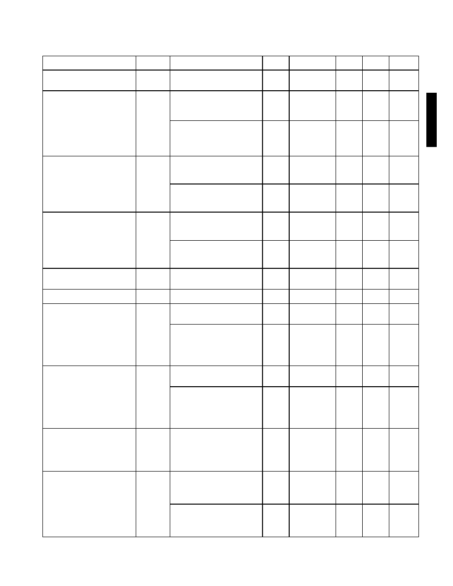
PIN CONNECTIONS
Jitter Peaking
Loop Bandwidth approximately
1.41MHz at 0.2UI input jitter
modulation
-
0.05
-
dB
4
Loop Bandwidth approximately
129kHz at 0.2UI input jitter
modulation
-
0.05
-
dB
4
Phaselock Unlock Timer
10nF PLCAP
-
67
-
µs
2, 4
NOTES
1. 100% Tested at 25∞C
2. Guaranteed by Design
3. Correlated Value
4. Using EB1515
AC ELECTRICAL CHARACTERISTICS (continued)
V
CC
= +5 V, T
A
= 0 ∞C to 70 ∞C unless otherwise specified
PARAMETER
SYMBOL
CONDITIONS
MIN
TYP
MAX
UNITS
NOTES
33
32
31
30
29
28
27
26
25
24
23
1
2
3
4
5
6
7
8
9
10
11
44 43 42 41 40 39 38 37 36 35 34
12 13 14 15 16 17 18 19 20 21 22
GS1515
TOP VIEW
NC
CD_V
CC
NC
R
SET
NC
CD_V
EE
NC
PD_V
EE
NC
NC
PD_V
CC
NC
LFS
NC
NC
LFA_V
EE
NC
NC
LFA_V
CC
NC
NC
LFA
DFT_V
EE
PLCAP
PLCAP
SHIELD
VCO
VCO
SHIELD
DDI_V
TT
DDI
DDI
SHIELD
LFS
BYPASS
PLL_LOCK
IJI
DM
DM
NC
SDO
NC
SDO
NC

522 - 23 - 01
5
G
S
1
515
PIN DESCRIPTIONS
NUMBER
SYMBOL
TYPE
DESCRIPTION
1, 3, 4, 6, 7, 9, 10,
24, 25, 27, 29, 31,
33, 34, 36, 38
NC
No connection. These pins are not bonded to the die.
2
LFS
INPUT
Loop filter capacitor connection.
5
LFA_V
EE
POWER
Most negative power supply connection - loop filter circuitry.
8
LFA_V
CC
POWER
Most positive power supply connection - loop filter circuitry.
11
LFA
OUTPUT
Control signal output: control voltage for the external GO1515 VCO.
12
DFT_V
EE
POWER
Most negative power supply connection - that enables the jitter demodulator
functionality, this pin should be connected to ground. If left floating, the DM
function is disabled resulting in a current saving of 340µA.
13, 14
PLCAP,
PLCAP
INPUT
Control signal input: PLL lock detect time constant capacitor connection.
15, 18, 22
SHIELD
No connect pins separating the DDI inputs, the VCO inputs and the loop filter
components to improve noise performance. Connection to be made to ground
in most cases depending upon PCB performance.
16, 17
VCO, VCO
INPUT
Control signal inputs: differential inputs for the external VCO. The GO1515 has
single ended output. In this case, the VCO input is decoupled to ground.
19
DDI_V
TT
INPUT
Centre tap of the two 50
on-chip termination resistors between the DDI and
the DDI inputs.
20, 21
DDI, DDI
INPUT
Differential inputs for the serial digital signals.
23
PD_V
CC
POWER
Most positive power supply connection - phase detector circuitry.
26
PD_V
EE
POWER
Most negative poser supply connection - phase detector circuitry.
28
CD_V
EE
POWER
Most negative power supply connection - cable driver circuitry.
30
R
SET
INPUT
Resistor used to set the serial digital output signal swing. It is connected
between here and ground with a very short trace length.
32
CD_V
CC
POWER
Most positive power supply connection - cable driver circuitry.
35, 37
SDO, SDO
OUTPUT
Differential serial digital outputs from the on-chip cable driver. These outputs
require 75
pull-up resistors.
39, 40
DM, DM
OUTPUT
Diagnostic signal: if the jitter demodulator function is not used, these pins must
be left floating.
41
IJI
OUTPUT
Status signal output: indicates the amount of excessive jitter on the incoming
DDI and DDI signals.
42
PLL_LOCK
OUTPUT
Status signal output: lock detect and carrier detect: PLL lock indicator output
used to indicate when the PLL is locked. This output is TTL compatible. When
the PLL_LOCK = LOW, the serial digital outputs are muted.
43
BYPASS
INPUT
Control signal input: operational TTL compatible input that controls whether the
input DDI and DDI signal is reclocked (BYPASS = HIGH) or is passed through
the device, unreclocked (BYPASS = LOW). Muting does not affect the
bypassed signal.
44
LFS
INPUT
Loop filter capacitor connection.