GENNUM CORPORATION P.O. Box 489, Stn. A, Burlington, Ontario, Canada L7R 3Y3
Tel. +1 (905) 632-2996 Fax. +1 (905) 632-5946 E-mail: info@gennum.com
www.gennum.com
Revision Date: August 2000
Document No. 522 - 26 - 00
PRELIMINARY DATA SHEET
G
S
1
522
FEATURES
∑ SMPTE 292M compliant
∑ 20:1 parallel to serial conversion
∑ NRZ(I) encoder & SMPTE scrambler with selectable
bypass
∑ NRZ to NRZ(I) serial data conversion
∑ 1.485Gb/s and 1.485/1.001Gb/s operation
∑ lock detect output
∑ selectable DUAL or QUAD 75
cable driver outputs
∑ 8 bit or 10 bit input data support
∑ 20 bit wide inputs
∑ 3.3V and 5V CMOS/TTL compatible inputs
∑ single +5.0V power supply
APPLICATIONS
SMPTE 292M Serial Digital Interfaces for Video Cameras,
Camcorders, VTR's, Signal Generators, Portable Equip-
ment, and NLE's.
DESCRIPTION
The GS1522 is a monolithic bipolar integrated circuit
designed to serialize SMPTE 274M and SMPTE 260M bit
parallel digital signals.
This device performs the following functions:
∑
Sync word mapping for 8-bit/10-bit operation.
∑
Parallel to Serial conversion of Luma & Chroma data
∑
Interleaving of Luma and Chroma data
∑
Data Scrambling (using the X
9
+X
4
+1 algorithm)
∑
Conversion of NRZ to NRZI serial data (using the (X+1)
algorithm)
∑
Selectable DUAL or QUAD 75
Cable Driver outputs
∑
Lock Detect Output
∑
1.485Gb/s or 1.485/1.001Gb/s operation
This device requires a single 5V supply and typically
consumes less than 1000mW of power while driving two
75
cables.
The GS1522 uses the GO1515 external VCO connected to
the internal PLL circuitry to achieve ultra low noise PLL
performance.
FUNCTIONAL BLOCK DIAGRAM
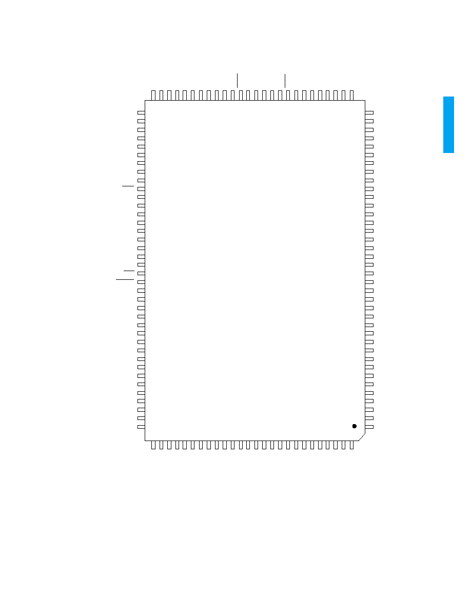
ORDERING INFORMATION
PART NUMBER
PACKAGE
TEMPERATURE
GS1522-CQR
128 pin MQFP
0∞C to 70∞C
SYNC DETECT
SMPTE
SCRAMBLER
INTERLEAVER
PARALLEL
TO SERIAL
CONVERTER
NRZ TO NRZI
PLL
INPUT
LATCH
GO1515
O/P0
O/P1
PLL_LOCK
SDO1_EN
R
SET1
SDO1-
SDO1+
SDO0-
SDO0+
R
SET0
BYPASS
RESET
SYNC_DETECT
_DISABLE
PCLK_IN
DATA_IN[19:0]
RESET
BYPASS
S
CLK
P
LOAD
MUTE
20
20
HD-LINX
TM
GS1522
HDTV Serial Digital Serializer
GENNUM CORPORATION
522 - 26 - 00
3
G
S
1
522
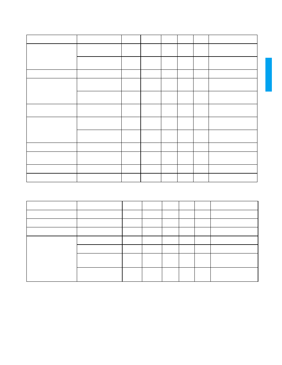
AC ELECTRICAL CHARACTERISTICS - PARALLEL TO SERIAL STAGE
V
DD
= 5V, T
A
= 0∞C to 70∞C unless otherwise specified.
PARAMETER
CONDITIONS
SYMBOL
MIN
TYP
MAX
UNITS
NOTES
Input Voltage Levels
V
IL
-
-
0.8
V
For compatibility with TTL
voltage levels
V
IH
2.0
-
-
V
For compatibility with TTL
voltage levels
Input Capacitance
C
IN
-
1
2
pF
Output Voltage Levels
V
OL
-
-
0.4
V
For compatibility with TTL
voltage levels
V
OH
2.4
-
-
V
For compatibility with TTL
voltage levels
Parallel Input Clock
Frequency
P
CLK_IN
-
74.25
-
MHz
74.25/1.001MHz also
Input Clock Pulse Width
Low
t
PWL
5
-
-
ns
Input Clock Pulse Width
High
t
PWH
5
-
-
ns
Input Clock Rise/Fall time
t
r
, t
f
-
500
1000
ps
20% to 80%
Input Clock Rise/Fall time
Matching
t
rfm
-
200
-
ps
Input Setup Time
t
SU
1.0
-
-
ns
Input Hold Time
t
IH
0
-
-
ns
DC ELECTRICAL CHARACTERISTICS
V
CC
= 5V, V
EE
= 0V, T
A
= 0∞C to 70∞C unless otherwise specified.
PARAMETER
CONDITIONS
SYMBOL
MIN
TYP
MAX
UNITS
NOTES
Positive Supply Voltage
Operating Range
V
CC
4.75
5.00
5.25
V
Power (system power)
V
CC
= 5.00V, T=25∞C
P
D
-
950
-
mW
(Driving two 75
outputs)
V
CC
= 5.00V, T=25∞C
P
D
-
1170
-
mW
(Driving four 75
outputs)
Supply Current
V
CC
= 5.25V, T=70∞C
-
-
300
mA
(Driving four 75
outputs)
V
CC
= 5.00V, T=25∞C
-
234
-
mA
(Driving four 75
outputs)
SDO1 disabled
V
CC
= 5.25V, 70∞C
-
-
240
mA
(Driving two 75
outputs)
SDO1 disabled
V
CC
= 5.0V, 25∞C
-
190
-
mA
(Driving two 75
outputs)
GENNUM CORPORATION
522 - 26 - 00
5
G
S
1
522
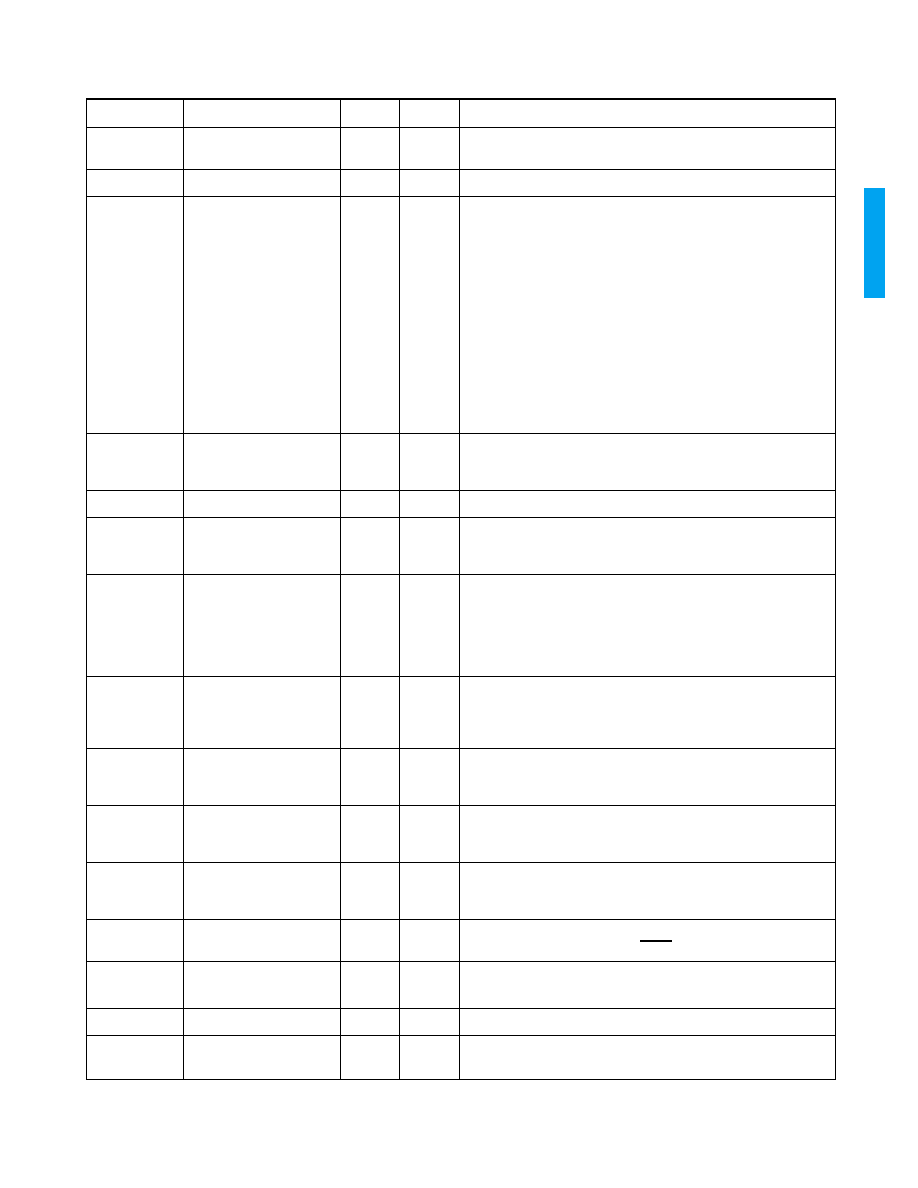
PIN DESCRIPTIONS
NUMBER
SYMBOL
LEVEL
TYPE
DESCRIPTION
1, 95
V
EE3
Power
Input
Negative Supply.
Most negative power supply connection, for
input stage.
2
PCLK_IN
TTL
Input
Parallel Data Clock
. 74.25 or 74.25/1.001MHz
3, 4, 5, 6, 7, 8,
9, 11, 12, 14,
19, 20, 32, 33,
34, 35, 36, 37,
38, 39, 40, 41,
42, 43,46, 50,
51, 52, 56, 60,
61, 62, 65, 66,
67, 68, 69, 70,
71, 72, 73, 80,
81, 83, 93, 97,
98, 99, 100,
101, 102, 108,
109, 116, 117,
120, 121
NC
No Connect
. These pins are not used internally. These pins
should be floating.
10
BUF_V
EE
Power
TEST
Negative Supply/Test Pin
. Most negative power supply
connection. For buffer for oscillator/divider for test purposes only.
Leave floating for normal operation.
13
XDIV20
TTL
TEST
Test Pin
. Test block output. Leave floating for normal operation.
15
PLL_LOCK
TTL
Output
Status Signal Output
. Indicates when the GS1522 is phase locked
to the incoming PCLK_IN clock signal. LOGIC HIGH indicates
PLL is in Lock. LOGIC LOW indicates PLL is out of Lock.
16
BYPASS
TTL
Input
Control Signal Input
. Used to bypass the scrambling function if
data is already scrambled by GS1501 or if non-SMPTE encoded
data stream such as 8b/10b is to be transmitted. When BYPASS is
LOW, the SMPTE scrambler and NRZ(I) encoder are enabled.
When BYPASS is HIGH, the SMPTE scrambler and NRZ(I) encoder
are bypassed.
17
RESET
TTL
Input
Control Signal Input
. Used to reset the SMPTE scrambler. For
logic HIGH; Resets the SMPTE scrambler and NRZ(I) encoder.
For logic LOW: normal SMPTE scrambler and NRZ(I) encoder
operation.
18, 26, 27, 28,
29, 30, 59
V
EE2
Power
Input
Negative Supply
. Most negative power supply connection. For
Cable Driver outputs and all other digital circuitry excluding input
stage and PLL stage.
21, 22, 23, 24,
25, 45, 57
V
CC2
Power
Input
Positive Supply
. Most positive power supply connection. For
Cable Driver outputs and all other digital circuitry excluding input
stage and PLL stage.
31
SDO1_EN
Power
Input
Control Signal Input
. Used to enable or disable the second serial
data output stage. This signal must be tied to GND to enable this
stage. Do not connect to a logic low.
44
R
SET1
Input
Control Signal Input
. External resistor is used to set the data
output amplitude for SDO1 and SDO1. Use a ±1% resistor.
47, 49
SDO1+, SDO1-
Analog
Output
Serial Data Output Signal
. Current mode serial data output #1.
Use 75
±1% pull up resistors to V
CC2
.
48, 54
SDO_NC
No Connect
. Not used internally. This pin must be left floating.
53, 55
SDO0+, SDO0-
Analog
Output
Serial Data Output Signal
. Current mode serial data output #0.
Use 75
± 1% pull up resistors to V
CC2
.