 | –≠–ª–µ–∫—Ç—Ä–æ–Ω–Ω—ã–π –∫–æ–º–ø–æ–Ω–µ–Ω—Ç: GS1524 | –°–∫–∞—á–∞—Ç—å:  PDF PDF  ZIP ZIP |

www.gennum.com
GS1524 HD-LINXTM II
Multi-Rate SDI Adaptive
Cable Equalizer
GS1524 Data Sheet
14976 - 7
June 2005
1 of 18
Key Features
∑
SMPTE 292M, SMPTE 344M and SMPTE 259M
compliant
∑
automatic cable equalization
∑
multi-standard operation from 143Mb/s to
1.485Gb/s
∑
supports DVB-ASI at 270Mb/s
∑
manual bypass (useful for low data rates with slow
rise/fall times)
∑
performance optimized for 270Mb/s and 1.485Gb/s
∑
typical maximum equalized length of Belden 1694A
cable: 140m at 1.485Gb/s, 350m at 270Mb/s
∑
50
differential output (with internal 50 pull-ups)
∑
Pb-free and RoHS Compliant
Key Specifications
∑
cable length indicator for SMPTE 259M inputs
∑
output mute based on max cable length adjust or
manual override
∑
single 3.3V power supply operation
∑
operating temperature range: 0∞C to +70∞C
Applications
∑
SMPTE 292M, SMPTE 344M and SMPTE 259M
Coaxial Cable Serial Digital Interfaces
Description
The GS1524 is a second-generation high-speed bipolar
integrated circuit designed to equalize and restore
signals received over 75
co-axial cable at data rates
from 143Mb/s up to 1.485Gb/s. The GS1524 is
designed to support SMPTE 292M, SMPTE 344M and
SMPTE 259M, and is optimized for performance at
270Mb/s and 1.485Gb/s.
The GS1524 features DC restoration to compensate for
the DC content of SMPTE pathological test patterns.
The GS1524 also incorporates a Cable Length Indicator
(CLI) that provides an indication of the amount of cable
being equalized for data rates up to 360Mb/s.
A voltage programmable mute threshold (MCLADJ) is
included to allow muting of the GS1524 output when an
approximate selected cable length is reached for
SMPTE 259M signals. This feature allows the GS1524
to distinguish between low amplitude SD-SDI signals
and noise at the input of the device. The CD/MUTE pin
provides an indication of the GS1524 mute status in
addition to functioning as a mute control input. The SD
outputs of the GS1524 may be forced to a mute state by
applying a voltage to the CD/MUTE pin.
Power consumption is typically 265mW using a 3.3V
power supply.
This component and all homogeneous subcomponents
are RoHS compliant.
Functional Block Diagram
CABLE LENGTH INDICATOR/ADJUSTOR
CARRIER DETECT
MUTE
EQUALIZER
DC RESTORE
OUTPUT
AGC
CLI
CD/MUTE
SDO
BYPASS
SDO
SDI
SDI
MCLADJ

GS1524 Data Sheet
14976 - 7
June 2005
2 of 18
Contents
Key Features.................................................................................................................1
Key Specifications.........................................................................................................1
Applications...................................................................................................................1
Description ....................................................................................................................1
1. Electrical Characteristics...........................................................................................3
1.1 Absolute Maximum Ratings ............................................................................3
1.2 DC Electrical Characteristics ..........................................................................3
1.3 AC Electrical Characteristics ...........................................................................4
2. Pin Out ......................................................................................................................6
2.1 Pin Connections ..............................................................................................6
2.2 Pin Descriptions ..............................................................................................6
3. Input/Output Circuits .................................................................................................8
4. Typical Performance Curves...................................................................................10
5. Detailed Description ................................................................................................14
6. Cable Length Indication/Carrier Detect/Mute ..........................................................15
7. Application Information............................................................................................16
7.1 PCB Layout ...................................................................................................16
7.2 Typical Application Circuit .............................................................................16
8. Package dimensions ...............................................................................................17
8.1 Ordering Information .....................................................................................17
9. Revision History ......................................................................................................18

GS1524 Data Sheet
14976 - 7
June 2005
3 of 18
1. Electrical Characteristics
1.1 Absolute Maximum Ratings
1.2 DC Electrical Characteristics
Parameter
Value
Supply Voltage
-0.5V to +3.6V
DC
Input ESD Voltage
500V
Storage Temperature Range
-50∞C< T
s
< 125∞C
Input Voltage Range (any input)
-0.3 to (V
CC
+ 0.3)V
Operating Temperature Range
0∞C to 70∞C
Power Dissipation
300mW
Lead Temperature (soldering, 10 sec.)
260∞C
Table 1-1: DC Electrical Characteristics
V
DD
= 3.3V, T
A
= 0∞C to 70∞C, unless otherwise shown
Parameter
Conditions
Symbol
Min
Typ
Max
Units
Notes
Test
Levels
Supply Voltage
≠
V
CC
3.135
3.3
3.465
V
± 5%
1
Power Consumption
T
A
=25∞C
P
D
≠
265
≠
mW
≠
5
Supply Current
T
A
=25∞C
S
≠
80
≠
mA
≠
1
Output Common Mode
Voltage
T
A
=25∞C
V
CMOUT
≠
V
CC
-
V
SDO
/2
≠
V
≠
7
Input Common Mode
Voltage
T
A
=25∞C
V
CMIN
≠
1.75
≠
V
≠
10
CLI DC Voltage (0m)
T
A
=25∞C
≠
≠
2.5
≠
V
≠
1
CLI DC Voltage (no signal)
T
A
=25∞C
≠
≠
1.9
≠
V
≠
7
Floating MCLADJ DC
Voltage
T
A
=25∞C
≠
≠
1.3
≠
V
≠
7
MCLADJ Range
T
A
=25∞C
≠
≠
0.69
≠
V
≠
7
CD/Mute Output Voltage
Carrier not
present
V
CD/Mute(OH)
2.6
≠
≠
V
≠
1
Carrier present
V
CD/Mute(OL)
≠
≠
1.2
≠
1

GS1524 Data Sheet
14976 - 7
June 2005
4 of 18
1.3 AC Electrical Characteristics
CD/Mute Input Voltage
Required to Force Outputs
to Mute
Min to Mute
V
CD/Mute
3.0
≠
≠
V
≠
7
CD/Mute Input Voltage
Required to Force Active
Max to Activate
V
CD/Mute
≠
≠
2.0
V
≠
7
TEST LEVELS
1. Production test at room temperature and nominal supply voltage with guardbands for supply and temperature ranges.
2. Production test at room temperature and nominal supply voltage with guardbands for supply and temperature ranges using
correlated test.
3. Production test at room temperature and nominal supply voltage.
4. QA sample test.
5. Calculated result based on Level 1, 2, or 3.
6. Not tested. Guaranteed by design simulations.
7. Not tested. Based on characterization of nominal parts.
8. Not tested. Based on existing design/characterization data of similar product.
9. Indirect test.
10.Wafer Probe
Table 1-1: DC Electrical Characteristics
V
DD
= 3.3V, T
A
= 0∞C to 70∞C, unless otherwise shown
Parameter
Conditions
Symbol
Min
Typ
Max
Units
Notes
Test
Levels
Table 1-2: AC Electrical Characteristics
V
DD
= 3.3V, T
A
= 0∞C to 70∞C, unless otherwise shown
Parameter
Conditions
Symbol
Min
Typ
Max
Units
Notes
Test
Levels
Serial input data rate
≠
≠
143
≠
1485
Mb/s
≠
6
Input Voltage Swing
T
A
=25∞C, differential
V
SDI
720
800
950
mV
p-p
0m cable
length
1
Output Voltage Swing
50
load, T
A
=25∞C,
differential
V
SDO
≠
750
≠
mV
p-p
≠
1
Maximum equalized
cable length
270Mb/s, Belden 1694A,
0.2UI output jitter
≠
≠
350
≠
m
Equalizer
Pathological
7
270Mb/s, Belden 8281
0.2UI output jitter
≠
≠
280
≠
m
Equalizer
Pathological
1
1.485Gb/s, Belden 1694A
0.25UI output jitter
≠
≠
140
≠
m
Equalizer
Pathological
7
1.485Gb/s, Belden 8281
0.25UI output jitter
≠
≠
100
≠
m
Equalizer
Pathological
1
Output Rise/Fall time
20% - 80%
≠
≠
80
220
ps
≠
1
Mismatch in rise/fall time
≠
≠
≠
30
ps
≠
1
GS1524 Data Sheet
14976 - 7
June 2005
5 of 18
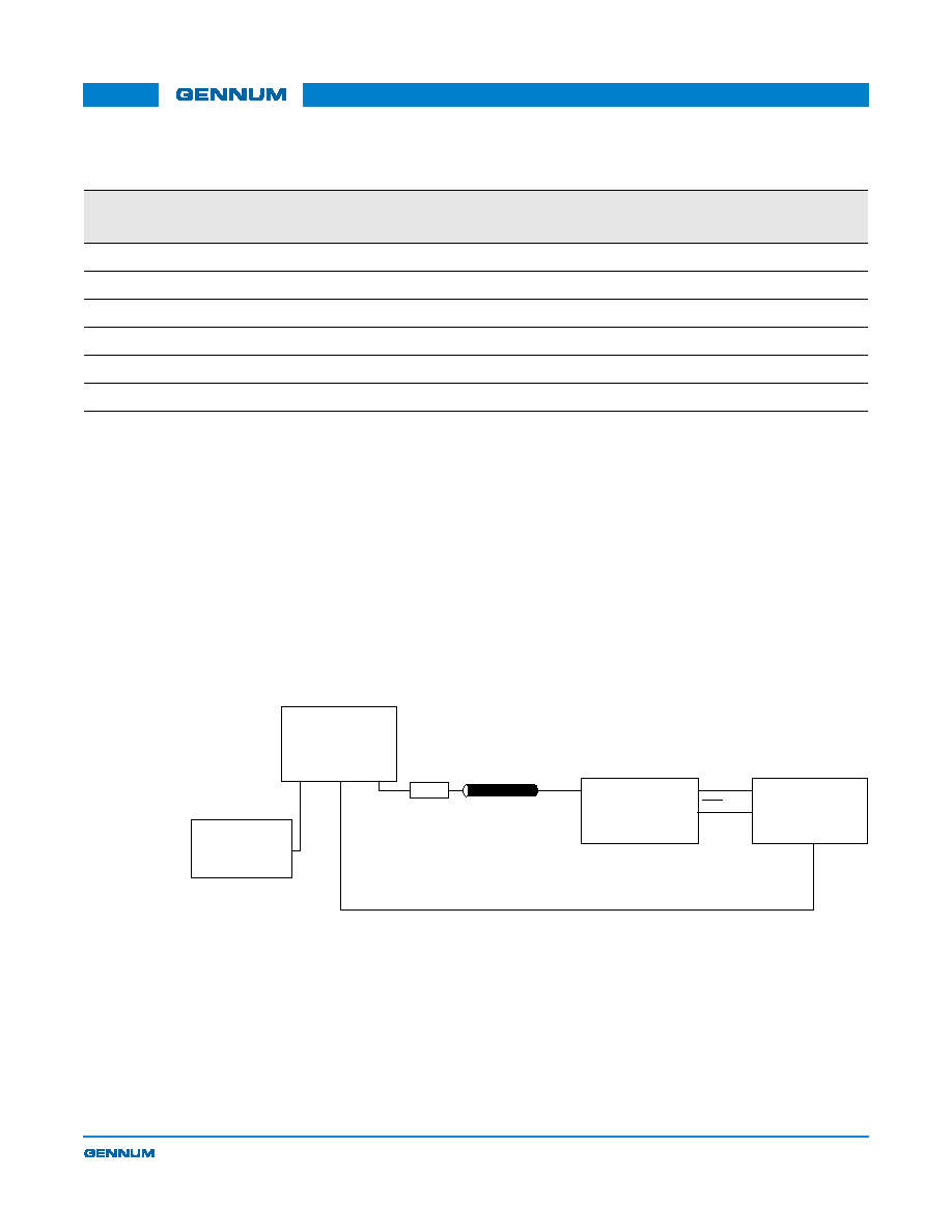
Figure 1-1: Test Circuit
Duty cycle distortion
≠
≠
≠
≠
30
ps
≠
1
Overshoot
≠
≠
≠
≠
10
%
≠
1
Input Return Loss
≠
≠
15
≠
≠
dB
1
7
Input Resistance
single ended
≠
≠
1.64
≠
k
≠
6
Input Capacitance
single ended
≠
≠
1
≠
pF
≠
6
Output Resistance
single ended
≠
≠
50
≠
≠
6
TEST LEVELS:
1. Production test at room temperature and nominal supply voltage with guardbands for supply and temperature ranges.
2. Production test at room temperature and nominal supply voltage with guardbands for supply and temperature ranges using
correlated test.
3. Production test at room temperature and nominal supply voltage.
4. QA sample test.
5. Calculated result based on Level 1, 2, or 3.
6. Not tested. Guaranteed by design simulations.
7. Not tested. Based on characterization of nominal parts.
8. Not tested. Based on existing design/characterization data of similar product.
9. Indirect test.
NOTES:
1. 1. Tested on CB1524 board from 5MHz to 2GHz.
Table 1-2: AC Electrical Characteristics
V
DD
= 3.3V, T
A
= 0∞C to 70∞C, unless otherwise shown
Parameter
Conditions
Symbol
Min
Typ
Max
Units
Notes
Test
Levels
GigaBERT
1400
EXT.
CLOCK
CLOCK
OUT
DATA
OUT
EXT.
CLOCK
1.485GHz/270MHz
GS1524
TEST BOARD
TDS 820
CH. 1
CH. 2
OUT
IN
OUT
EXT. TRIGGER
50/75
8281 or 1694A CABLE