FEATURES
∑ incorporates GR504, 3 stage amplifer chip
∑ designed to drive class D integrated receivers
∑ adjustable symmetrical peak clipper for MPO
control
∑ two low noise inverting preamplifiers
∑ mid-supply referenced output stage
∑ anti-aliasing filter network
STANDARD PACKAGING
∑ Hybrid Typical Dimensions:
0.244 in x 0.102 in x 0.115 in
(6.20 mm x 2.59 mm x 2.92 mm)
DESCRIPTION
The GS3018 contains Gennum's GR504 class D preamplifier
chip, six capacitors and one resistor. Capacitor C1 on the
hybrid, in conjunction with R
MIC
on the GR504 chip, form a
high pass filter which provides a very well regulated supply
voltage for the microphone. Resistor R1, capacitor C2 and
the output impedance of the microphone (
4 k
) also form
a high pass filter with a corner frequency of approximately
240 Hz.
GS3018 - HYB DATA SHEET
Provisions have been made on the hybrid to allow the
manufacturer to increase or decrease this corner frequency
with the addition of a capacitor. As the class D receiver
utilizes a 100 kHz clock, lower harmonics of the frequency
may feed back into the system and interact with the
incoming signal from the microphone. Capacitors C5 and
C6 have been added to the hybrid to minimize this effect,
known as "aliasing".
Blocks A and B on the GR504 are low noise inverting
preamplifiers with an open loop voltage gain of typically
50 dB. Typically, the volume control potentiometer would
be placed around block A, and block B used either as a
Gain Trim stage or as a Telecoil amplifier. The voltage gain
of these two blocks is determined by the ratio of the input
resistance to the value of the feedback resistor. With
100 k
potentiometer used as a feedback resistor for both
stages, block A would have a maximum gain of 20 dB, and
block B a gain of 26 dB.
Block C is a mid-supply referenced output stage designed
to drive class D receivers. It is typically capable of 670 mV
peak to peak output voltage swing and 14 dB of MPO
(Maximum Power Output) control with a 10 k
MPO
potentiometer. The gain of the output stage is fixed at
typically 16 dB.
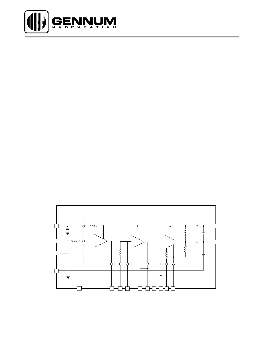
FUNCTIONAL BLOCK DIAGRAM
GR504
GS3018
VC1
VC2
B
OUT1
B
OUT2
V
MIC
R
MIC
GND
OUT
-
MGND
5k
B
A
C2
47n
C1
4µ7
R1
10k
V
B
MPO
C
IN
C5
1n8
C6
1n8
C3
68n
C4
68n
R
P1
R
P2
C3
B
RIN
B
IN
IN
C2
4
2
3
1
13
7
7
5
5
6
6
- C
10
9
9
8
8
16
11
12
14
15
4
2
3
2A
1
10
-
All resistors in ohms, all capacitors
in farads unless otherwise stated.
Class D Preamp with
Anti-Aliasing Network
Revision Date: May 1998
Document No. 521 - 09 - 03
GENNUM CORPORATION P.O. Box 489, Stn. A, Burlington, Ontario, Canada L7R 3Y3 tel. +1 (905) 632-2996
Web Site: www.gennum.com E-mail: hipinfo@gennum.com

521 - 09 - 03
2
PARAMETER
SYMBOL
CONDITIONS
MIN
TYP
MAX
UNITS
Supply Current
I
AMP
165
240
315
µ
A
STAGE A AND B
Input Bias Voltage
V
BIAS
500
580
650
mV
Gain (pin 2 to pin 8)
GAIN
AB
V
IN
= -60dBV
40
44
48
dB
OUTPUT STAGE
Input Bias Voltage
V
CIN
550
612
670
mV
Voltage Gain (pin 15 to pin 10)
GAIN
C
V
IN
= -50dBV, R
MPO
= 0
14
16
18
dB
Maximum Output Level
MPO
V
IN
= -22dBV, R
MPO
= 0
-14.5
-12.5
-10.5
dBV
MPO Range
MPO
V
IN
= -22dBV, R
MPO
= 10K
12
14
16
dB
Gain at 10 kHz
GAIN
10kHz
V
IN
= -55dBV, R
MPO
= 0
0
4.5
9.0
dB
All parameters and switches remain as shown in the Test Circuit unless otherwise stated in CONDITIONS column
V
QX
- quiescent (unbias) voltage measured on the pin, (nothing connected to the pin). V
PX
- actual voltage measured on the pin at given
condition (X is pin number).
PAD CONNECTION
CAUTION
CLASS 1 ESD SENSITIVITY
ABSOLUTE MAXIMUM RATINGS
PARAMETER
VALUE / UNITS
Supply Voltage
3 VDC
Power Dissipation
25 mW
Operating Temperature Range
-10
∞
C to 40
∞
C
Storage Temperature Range
-20
∞
C to 70
∞
C
Conditions: Frequency = 1 kHz, Temperature = 25
∞
C, Supply Voltage V
B
= 1.3 V
ELECTRICAL CHARACTERISTICS
9
3
2
1
1 4
11
4
5
6
7
8
9
10
I N
MGND
C2
BRIN
VC1
VC2
BOUT2
VB
OUT
CIN
C3
GND
MPO
BIN
BOUT1
VMIC
16
1 5
12
13
521 - 09 - 03
3
100k
100k
1kHz
0µ1
50k
1.3VDC
V
IN
V
IN
GR504
GS3018
R
MIC
-
5k
B
A
C1
4µ7
R
MPO
C5
1n8
C6
1n8
C3
68n
C4
68n
R
P1
R
P2
3kHz
4
2
1
13
7
7
5
5
6
6
- C
9
9
8
8
16
11
12
14
15
4
2
3
1
10
2A
-
3
10
C2
47n
R1
10k
All resistors in ohms, all capacitors
in farads unless otherwise stated.
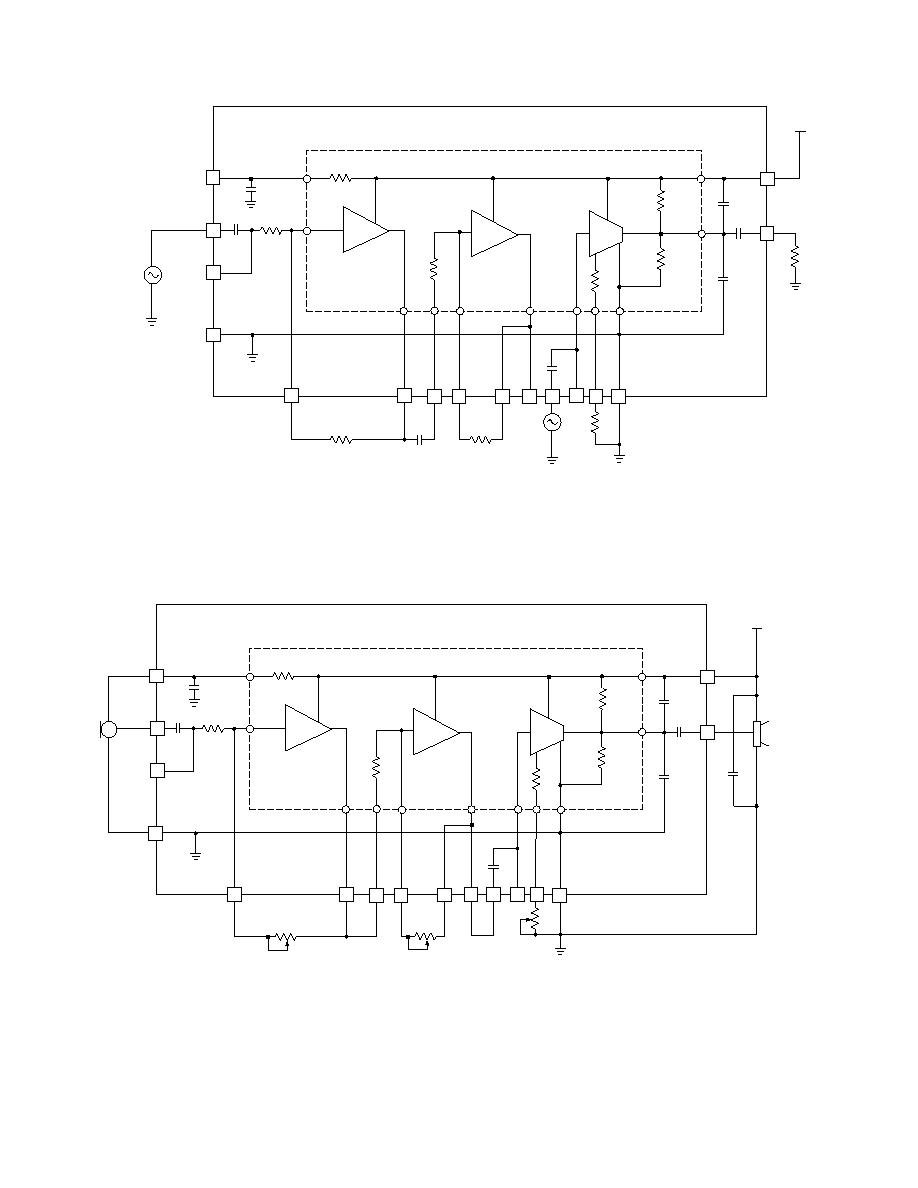
Fig. 2 Typical Hearing Instrument Application
1µ
GR504
GS3018
MIC
R
MIC
-
5k
B
A
C1
4µ7
C5
1n8
C6
1n8
C3
68n
C4
68n
R
P1
R
P2
4
2
3
1
13
7
7
5
5
6
6
- C
10
9
9
8
8
16
11
12
14
15
4
2
3
1
2A
10
-
R
VC
100k
R
GT
100k
1.3VDC
R
MPO
10k
CLASS D
INTEGRATED
RECEIVER
C2
47n
R1
10k
All resistors in ohms, all capacitors
in farads unless otherwise stated.
Fig. 1 Production Test Circuit
521 - 09 - 03
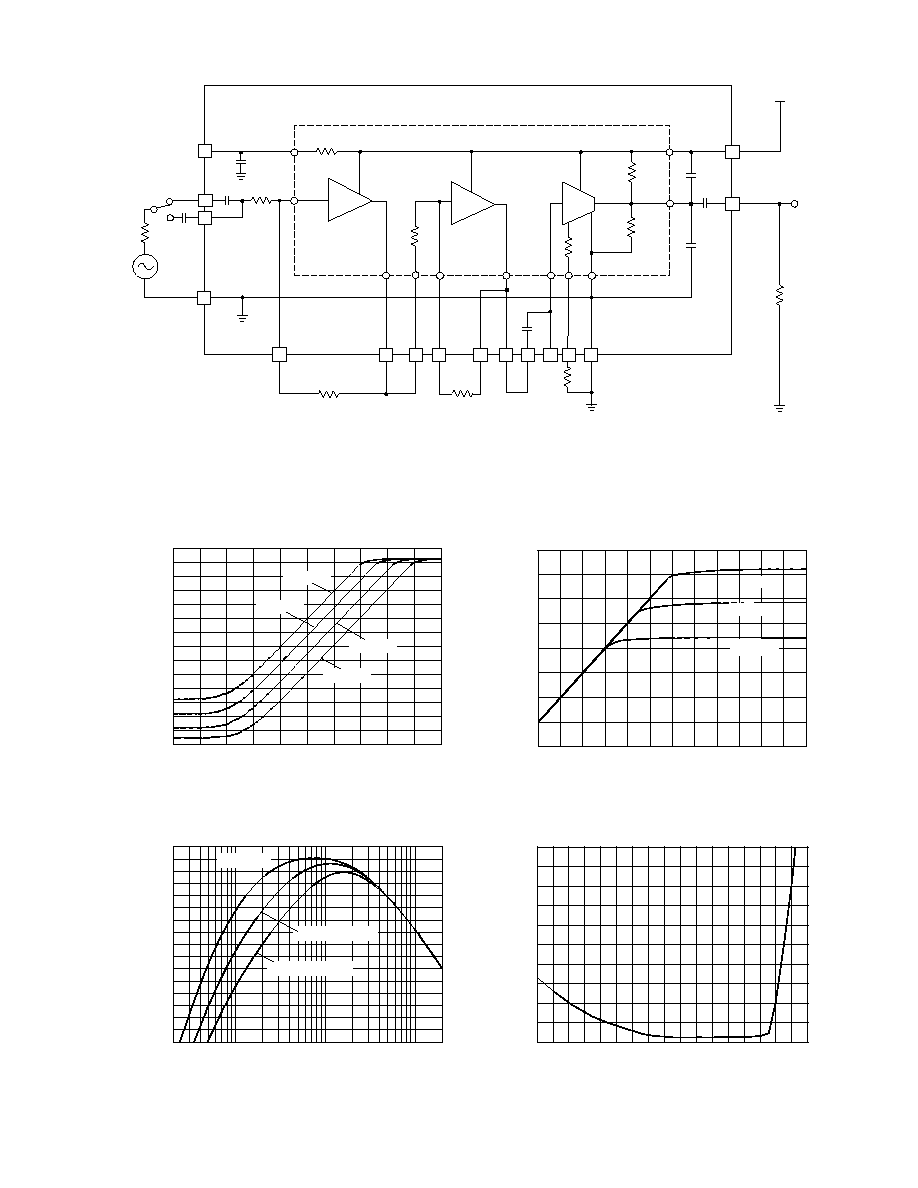
5
Fig. 8 Frequency Response vs C
IN
Fig. 9 THD vs Input (R
FA
=100k, R
MPO
=0)
50k
GR504
GS3018
R
MIC
-
5k
B
A
C1
4µ7
C5
1n8
C6
1n8
C3
68n
C4
68n
R
P1
V
OUT
R
P2
4
2
3
V
IN
1kHz
C
EXT
3k9
a
b
1
13
7
7
5
5
6
6
- C
10
9
9
8
8
16
11
12
14
15
4
2
3
1
2A
10
-
R
FA
100k
R
FB
100k
1.3VDC
R
MPO
C2
47n
R1
10k
S1
Fig. 5 Characterization Circuit
(used to generate typical curves)
All resistors in ohms, all capacitors
in farads unless otherwise stated.
C
EXT
=22nF(S1=b)
C
EXT
=10nF(S1=b)
20
100
1k 10k 20k
FREQUENCY (Hz)
-100 -96 -92 -88 -84 -80 -76 -72 -68
INPUT (dBV)
OUTPUT (dBV)
-140 -130 -120 -110 -100 -90 -80 -70 -60 -50 -40
INPUT (dBV)
R
FA
=100k
R
FA
=47k
R
FA
=22k
R
FA
=10k
Fig. 6 Input vs Output (R
MPO
= 0)
-100 -90 -80 -70 -60 -50 -40
INPUT (dBV)
Fig. 7 Maximum Power Output vs R
MPO
R
MPO
=0
R
MPO
=3k3
OUTPUT (dBV)
-10
-15
-20
-25
-30
-35
-40
-45
-50
-10
-20
-30
-40
-50
-60
-70
-80
2
-2
-6
-10
-14
-18
-22
-26
-30
RELATIVE OUTPUT (dB)
10
9
8
7
6
5
4
3
2
1
0
THD (%)
47nF(S1=a)
R
MPO
=10k
