 | –≠–ª–µ–∫—Ç—Ä–æ–Ω–Ω—ã–π –∫–æ–º–ø–æ–Ω–µ–Ω—Ç: GS3021 | –°–∫–∞—á–∞—Ç—å:  PDF PDF  ZIP ZIP |

FEATURES
∑ designed to drive class D integrated receivers
∑ handles high input levels (up to 100 mVRMS) cleanly
∑ low THD and IMD distortion
∑ unique twin average detectors
∑ dual channel signal processing
∑ adjustable AGC threshold levels
∑ MPO range externally adjustable
∑ highpass filter with adjustable corner frequency
∑ 2:1 compression of high frequencies
∑ no external capacitors or resistors required
∑ 30% smaller by volume than DynamEQ
Æ
I (GS3011)
STANDARD PACKAGING
∑ Hybrid Typical Dimensions
0.250 in x 0.115 in x 0.115 in
(6.35 mm x 2.92 mm x 2.92 mm)
DESCRIPTION
The DynamEQ
Æ
I hybrid is a dynamically adaptive loudness
growth equalizer. Its gain and frequency response is
dependent on the user's environment, and is designed
for level dependant frequency response providing treble
increase at low levels (TILL). The unique twin averaging
detector circuit dramatically reduces pumping effects
and is optimized for mild to moderate hearing loss.
DynamEQ
Æ
I has two signal paths for dual channel
processing incorporating 4 amplifying stages (A , B,
C, D) and the AGC processing circuit.
Stage A is a highpass channel with 2:1 compression,
Stage B is a wideband unity gain buffer. The sum of the
two paths gives a high frequency boost to low level
signals, which gradually compresses to a flat response at
high input levels. Stage C is used for volume control
adjustment, while stage D is a fixed gain stage with MPO
control designed to drive class D integrated receivers.
OUT
0µ1
100k
- C
V
B
V
REG
C1
2µ2
10
REGULATOR
SLOW
AVERAGE
DETECTOR
FAST
AVERAGE
DETECTOR
R
TH
CURRENT
REFERENCE
2:1
COMPRESSION
CONTROL
GS3021
MPO
C
HP
IN
MGND
C
OUT
C
IN
0µ1
0µ1
12k
C3
0µ1
C2
3n9
- A
- B
R1
68k
RECTIFIER
D
R2
50k
GND
50k
2µ2
100k
50k
50k
48k
48k
C6
C7
V
B
C4
C5
9
1
11
8
4
7
6
2
3
5
DynamEQ
Æ
I
Dynamic Equalizer - Class D
GS3021 - DATA SHEET
FUNCTIONAL BLOCK DIAGRAM
All resistors in ohms, all capacitors in farads unless otherwise stated.
Patent Pending.
Revision Date: May 1998
Document No. 521 - 06 - 03
GENNUM CORPORATION P.O. Box 489, Stn. A, Burlington, Ontario, Canada L7R 3Y3 tel. +1 (905) 632-2996
Web Site: www.gennum.com E-mail: hipinfo@gennum.com

521 - 06 - 03
2
PARAMETER
SYMBOL
CONDITIONS
MIN
TYP
MAX
UNITS
Hybrid Current
I
AMP
V
IN
= 0V
RMS
, R
MPO
= 50k
120
230
380
µ
A
Minimum Voltage
V
B
1.1
-
-
V
Total Harmonic Distortion
THD
R
VC
= 15k
; V
IN
= -40dBV at1kHz
-
0.1
1
%
Input Referred Noise
IRN
NFB 0.2 to 10kHz at 12dB/oct
-
2.5
-
µ
V
RMS
Total System Gain
A
V
45
48
51
dB
AGC
Compression Ratio
COMP
V
IN
= -60dBV and -80dBV
1.74:1
1.95:1
2.11:1
Ratio
Threshold
-
-94
-
dBV
Compression Gain Range
A
RANGE
R
VC
= 10k
; Note 1
26
28
-
dB
High Pass Corner Frequency
HPC
C
HP
- Not Connected
-
3.4
-
kHz
System Gain in Compression
A
80
V
IN
= -80dBV
38
40
42
dB
OUTPUT STAGE
Maximum Output Level
MPO
V
IN
= -20dBV,
R
MPO
= 0
-14.3
-12.3
-10.3
dBV
MPO Range
MPO
V
IN
= -20dBV,
R
MPO
= 0 to 50k
13.8
15.8
17.8
dB
REGULATOR
Regulator Voltage
V
REG
0.89
0.94
0.99
V
All parameters and switches remain as shown in the Test Circuit unless otherwise stated in CONDITIONS column
V
PX
actual voltage measured on the pin at given condition (X is pin number)
CAUTION
CLASS 1 ESD SENSITIVITY
ABSOLUTE MAXIMUM RATINGS
PARAMETER
VALUE / UNITS
Supply Voltage
3 VDC
Power Dissipation
25 mW
Operating Temperature Range
-10
∞
C to 40
∞
C
Storage Temperature Range
-20
∞
C to 70
∞
C
PAD CONNECTION
Conditions: Input Level V
IN
= -97dBV, Frequency = 5 kHz, Temperature = 25
∞
C, Supply Voltage V
B
= 1.3 V
ELECTRICAL CHARACTERISTICS
1
2
3
4
5
6
7
8
9
10
11
C
OUT
MGND
R
TH
MPO
OUT
CHP
V
REG
GND
V
B
C
IN
IN
Notes:
1.
A
RANGE
= V
P3
[V
IN
= -97dBV] - V
P3
[V
IN
= -20 dBV] + 77dBV
521 - 06 - 03
3
EK3024
or
MODEL 39
0µ1
2µ2
R
VC
100k
1.3V
EP3074
1.3V
100k
- C
C1
2µ2
10
REGULATOR
SLOW
AVERAGE
DETECTOR
FAST
AVERAGE
DETECTOR
CURRENT
REFERENCE
2:1
COMPRESSION
CONTROL
GS3021
0µ1
0µ1
12k
C3
0µ1
C2
3n9
- A
- B
R1
68k
RECTIFIER
D
R2
50k
50k
2µ2
100k
50k
50k
C6
C7
V
B
C4
C5
9
1
11
8
4
7
2
3
5
6
0µ1
48k
48k
All resistors in ohms, all capacitors in farads unless otherwise stated.
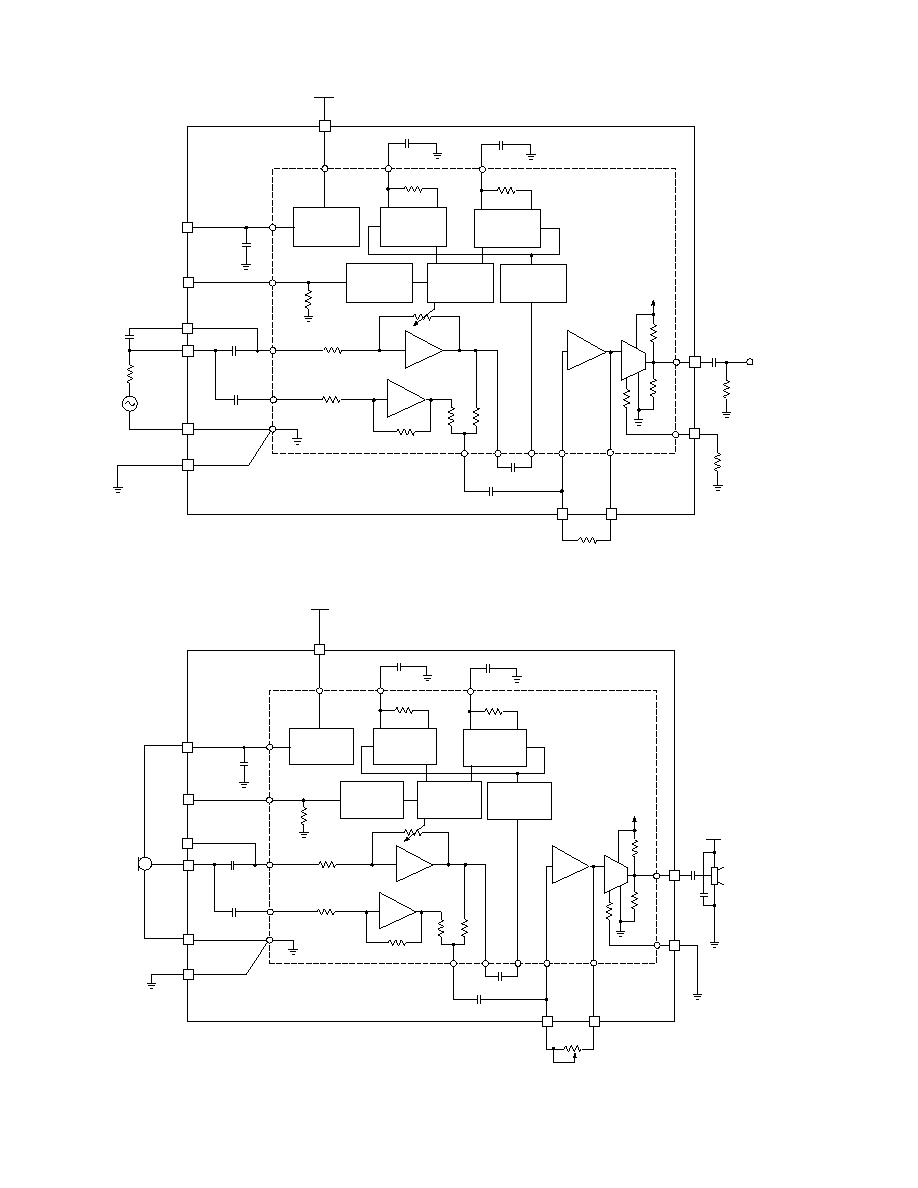
Fig.1 Production Test Circuit
R
VC
100k
R
MPO
=0
0µ1
GS3021
1.3V
0µ1
100k
- C
C1
2µ2
10
REGULATOR
SLOW
AVERAGE
DETECTOR
FAST
AVERAGE
DETECTOR
CURRENT
REFERENCE
2:1
COMPRESSION
CONTROL
0µ1
0µ1
C4
C5
12k
C3
0µ1
C2
3n9
R1
68k
RECTIFIER
D
R2
50k
50k
2µ2
100k
50k
50k
C6
C7
V
B
9
1
11
8
4
7
6
2
3
5
V
IN
3k9
C
HP
=0µ1
- B
- A
50k
48k
48k
All resistors in ohms, all capacitors in farads unless otherwise stated.
Microphones and receivers shown above are for illustrative purposes only.
Manufacturers can design with other appropriate transducers.
Fig. 2 Example of Hearing Instrument Application

521 - 06 - 03
4
R
VC
15k
V
IN
3k9
CHP
(Normally not
connected)
1.3V
R
TH
=
0µ1
100k
- C
C1
2µ2
10
REGULATOR
SLOW
AVERAGE
DETECTOR
FAST
AVERAGE
DETECTOR
CURRENT
REFERENCE
2:1
COMPRESSION
CONTROL
GS3021
0µ1
0µ1
12k
C3
0µ1
C2
3n9
- A
- B
R1
68k
RECTIFIER
D
R2
50k
50k
2µ2
100k
50k
50k
C6
C7
V
B
50k
0µ1
C4
C5
9
1
11
8
4
7
6
2
3
5
48k
48k
VOLUME
CONTROL
BATTERY
EP3074
0µ1
R
MPO
+
+
+
-
1
2
3
4
5
6
7
8
9
10
11
MIC
REC
2µ2
EK3024
or
MODEL 39
All resistors in ohms, all capacitors in farads unless otherwise stated.
Fig. 4 Characterization Circuit (used to generate typical curves)
Microphones and receivers shown above are for illustrative purposes only.
Manufacturers can design with other appropriate transducers.
Fig. 3 Example of Assembly Diagram

521 - 06 - 03
5
FREQUENCY (Hz)
Fig. 7 Frequency Response for Different R
VC
Values
R
TH
=
= 100k
= 47k
= 22k
= 0
V
IN
=-96dBV
20
100
1k 10k 20k
FREQUENCY (Hz)
Fig. 10 Frequency Characteristics for Different
R
TH
Values
V
IN
=-40dBV
= 5kHz
1kHz
2kHz
5kHz
20 100 1k 10k 20k
FREQUENCY (Hz)
Fig. 5 Frequency Response for Different Input Levels
V
IN
=-60dBV
R
TH
=
20
100
1k
10k 20k
FREQUENCY (Hz)
Fig. 8 Corner Frequency vs C
HP
Capacitor Value
V
IN
=-96dBV
R
TH
= 0
22k
47k
100k
R
TH
=
35
30
25
20
15
10
5
0
-5
-10
-15
V
IN
=-20dBV
V
IN
=-80dBV
V
IN
=-88dBV
V
IN
=-96dBV
1kHz
2kHz
5kHz
R
TH
= 0
V
IN
= -50dBV
R
VC
=100k
20 100 1k 10k 20k
R
VC
=47k
R
VC
=22k
R
VC
=15k
V
IN
=-70dBV
-10
-20
-30
-40
-50
-60
-70
-80
-90
-100 -90 -80 -70 -60 -50 -40 -30 -20 -10 0
INPUT LEVEL (dBV)
Fig. 6 I/O Transfer Function for Different Test
Frequencies. Shown for Min/Max R
TH
Resistors Values
30
25
20
15
10
5
0
-5
-10
-15
35
30
25
20
15
10
5
0
-5
-10
-15
-10
-20
-30
-40
-50
-60
-70
-80
-90
-100 -90 -80 -70 -60 -50 -40 -30 -20 -10 0
INPUT LEVEL (dBV)
Fig. 9 I/O Transfer Function for Different R
TH
Resistors
35
30
25
20
15
10
5
0
-5
-10
-15
C
HP
=100nF
C
HP
=68nF
C
HP
=33nF
C
HP
=10nF
C
HP
=No Capacitor
V
IN
=-20dBV
OUTPUT LEVEL (dBV)
GAIN (dB)
OUTPUT LEVEL (dBV)
GAIN (dB)
GAIN (dB)
GAIN (dB)

521 - 06 - 03
6
1
0.1
1
0.1
10
Fig. 12 THD & Noise vs Input Level
1
0.1
Fig. 14 Intermodulation Distortion (CCIF)
vs Level
R
MPO
=0
R
MPO
=10k
R
MPO
=50k
-50 -45 -40 -35 -30 -25 -20 -15 -10 -5 0
INPUT LEVEL (dBV)
Fig. 11
I
/O for Various R
MPO
Settings
No Capacitor
CHP=0.1
µ
F
-80 -70 -60 -50 -40 -30 -20
INPUT LEVEL (dBV)
No Capacitor
CHP=0.1
µ
F
-80 -70 -60 -50 -40 -30 -20
INPUT LEVEL (dBV
3k
10k 100k
FREQUENCY (Hz)
Fig. 15 Intermodulation Distortion (CCIF)
vs Frequency
100
1k 10k
FREQUENCY (Hz)
Fig. 13 THD & Noise vs Frequency
CHP=0.1
µ
F
No Capacitor
=1kHz
V
IN
=-40dBV
10
1
0.1
V
IN
=-40dBV
=200Hz
-12
-14
-16
-18
-20
-22
-24
-26
-28
-30
-32
-34
-36
-38
-40
R
MPO
=33k
R
MPO
=22k
= 5kHz
=200Hz
No Capacitor
CHP=0.1
µ
F
=4kHz
OUTPUT (dBV)
IMD (%)
THD & NOISE (%)
IMD (%)
THD & NOISE (%)
521 - 06 - 03
7
GS3021
XXXXXX
0.125 MAX
(3.18)
C1
C7
1
2
3
4
5
6
7
8
9
10
11
0.115
(2.92)
0.250
(6.35)
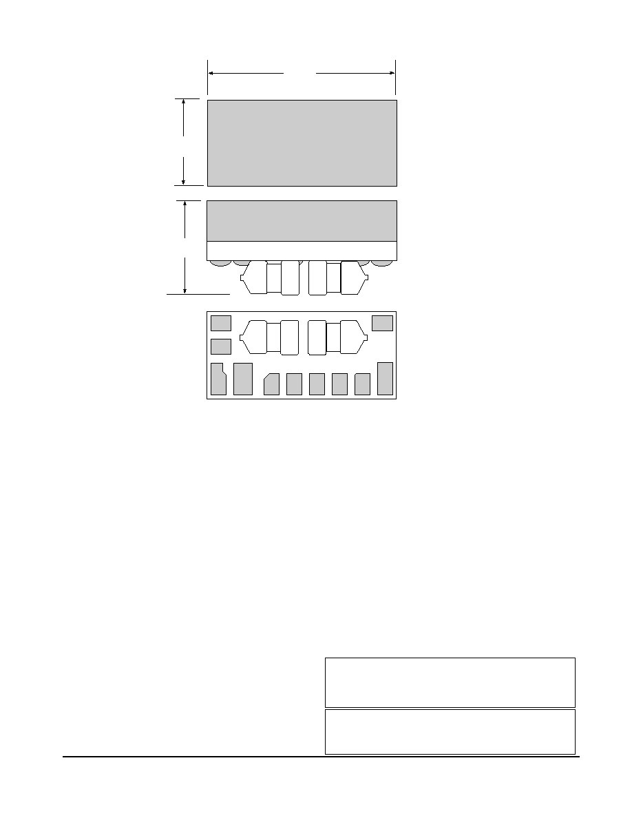
Dimension units are in inches.
Dimensions in parenthesis are in millimetres converted
from inches and include minor rounding errors.
1.0000 inches = 25.400 mm.
Dimension
±
0.005 (+0.13) unless otherwise stated.
Pad numbers for illustration purposes only.
Smallest pad 0.020 x 0.027 (0.51 x 0.69)
Largest pad 0.025 x 0.041 (0.64 x 1.04)
XXXXXX - work order number.
This hybrid is designed for point to point manual soldering.
Fig. 16 Hybrid Layout & Dimensions
DOCUMENT IDENTIFICATION:
DATA SHEET
The product is in production. Gennum reserves the right to make
changes at any time to improve reliability, function or design, in
order to provide the best product possible.
Gennum Corporation assumes no responsibility for the use of any circuits described herein and makes no representations that they are free from patent infringement.
© Copyright December 1993 Gennum Corporation. All rights reserved. Printed in Canada.
REVISION NOTES:
Updated to Data Sheet