 | –≠–ª–µ–∫—Ç—Ä–æ–Ω–Ω—ã–π –∫–æ–º–ø–æ–Ω–µ–Ω—Ç: GS563 | –°–∫–∞—á–∞—Ç—å:  PDF PDF  ZIP ZIP |
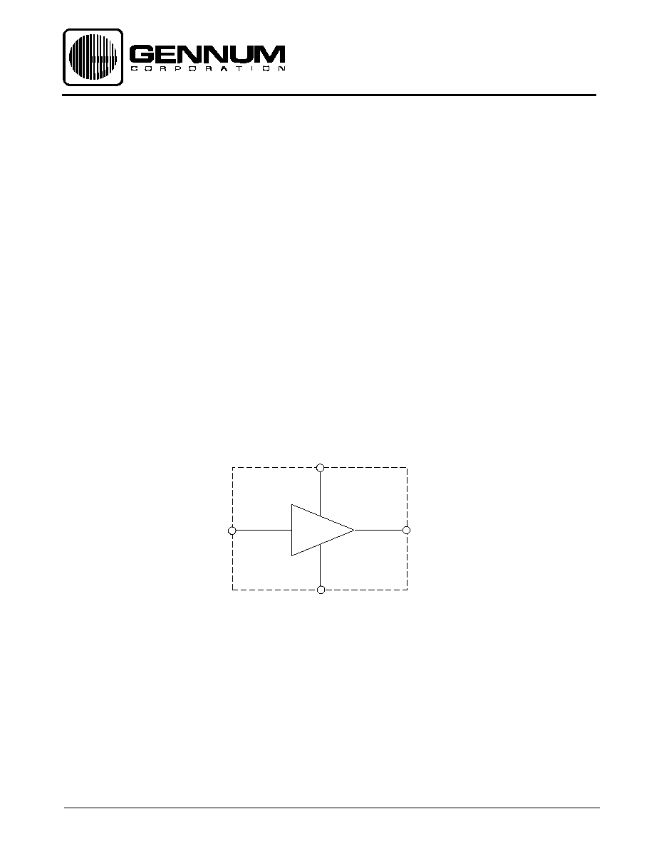
Single Stage
Inverting Amplifier
GS563 - DATA SHEET
FEATURES
∑ 1.0 to 5 VDC operating range
∑ low current consumption (54
µ
A)
∑ 1% electrical distortion
∑ typically 55 dB open loop gain
∑ low pin count (4 pin)
∑ ideal for active filtering
DESCRIPTION
T
he GS563 is a low noise, low current, inverting amplifier which
utilizes Gennum's low voltage bipolar JFET technology.
The amplifier has a minimum open loop gain of 45 dB with the
closed loop gain set by the ratio of feedback resistor to the
input resistor. For a well controlled gain tolerance, it is
recommended that the closed loop gain be at least 20 dB
below the open loop gain.
The device is internally bias compensated, preventing any DC
current flow via external feedback resistors. It is ideally suited
for filtering applications and can be used as a drop in
replacement for single transistor configurations.
FUNCTIONAL BLOCK DIAGRAM
OUTPUT
V
CC
INPUT
GS563
3
7
2
6
GND
STANDARD PACKAGING
∑ 8 pin PLID
Æ
∑ Chip size 27 x 25 mils
Document No. 520 - 67 - 01
Revision Date: May 1998
GENNUM CORPORATION P.O. Box 489, Stn. A, Burlington, Ontario, Canada L7R 3Y3 tel. +1 (905) 632-2996
Web Site: www.gennum.com E-mail: hipinfo@gennum.com

2
520 - 67 - 01
R
F =
1M
10µA
R1
1k
680pF
C1
1.0
V
IN
R
S
3k92
V
OUT
R2
10
a
b
c
S1
a
b
c
d
a
b
c
1µA
V
CC
1.3V
1µF
S3
V
10µA
S2
R
F
= 392k
180mV
RMS
at 1kHz
0.4V
DC
+
A
GS563
6
2
7
3
PARAMETER
SYMBOL
CONDITIONS
MIN
TYP MAX
UNITS
Amplifier Current
I
AMP
30
54
80
µ
A
Bias Voltage (Pin 3)
V
Q3
475
550
675 mV
Bias Current (Pin 3)
I
BIAS
See Note 1
-50
0
50 nA
Output Voltage
V
OH
S1 = c, S2 = b, S3 = b
200
590
-
mV
Swing - High (Pin 3)
See Note 2
Output Voltage
V
OL
S1 = b, S2 = b, S3 = c
200
258
-
mV
Swing - Low (Pin 3)
See Note 3
Open Loop Gain
A
OL
S1 = d, S2 = c, See Note 4
45
55
-
dB
Input Referred Noise
I.R.N.
Aweight S1 = d, S2 = c
-
1.0
2.5
µ
V
Distortion
THD
S1 = d, S2 = c, V
OUT
<100 mV
RMS
-
0.64
1.0
%
Supply Rejection
P
SRR
Open Loop
6
11
-
dB
All switch positions remain as shown in Test Schematic unless otherwise stated. V
P
is the actual voltage measured on the pin at given condition.
V
Q
- quiescent (unbias) voltage measured on the pad (nothing connected to the pin)
Note: 1.
I
BIAS
= (V
P3
[S2 = b] - V
Q3
) /1M
2.
V
OH
= V
P6
- V
Q6
3.
V
OL
= V
Q6
- V
P6
4.
A
OL
= 20 log (1 + R
F
/ R
S
) - (20 log ( (R
F
/ R
S
) (1 / (1 + R1 / R2) ) (V
IN
/ V
OUT
) - 1) )
ELECTRICAL CHARACTERISTICS
Stage = 1.3V Temperature = 25
o
C
Fig. 1 GS563 Test Circuit
PIN CONNECTIONS
ABSOLUTE MAXIMUM RATINGS
PARAMETER
VALUE / UNITS
Supply Voltage
5V DC
Power Dissipation
25 mW
Operating Temperature
-10
o
to +40
o
C
Storage Temperature
-20
o
to +70
o
C
CAUTION
CLASS 1 ESD SENSITIVITY
All resistors in ohms, all capacitors
in farads unless otherwise stated.
V
CC
OUT
GND
IN
1
4
5
8
3
520 - 67 - 01
BASE CURRENT
COMPENSATION
6
2
7
3
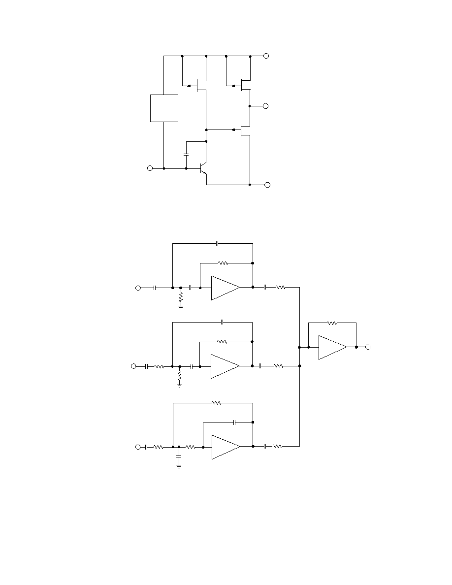
Fig. 2 Functional Schematic
V1
V2
R3
R2
R6
C3
R1
C1
C2
C4
V
O
C5
R4
R5
C6
C7
R7
C8
R10
C11
C12
R11
R8
R9
C10
C9
V3
R11
BAND PASS
LOW PASS
HIGH PASS
All resistors in ohms, all capacitors in farads unless otherwise stated.
(For Filter Design refer to Note 600-9, Active Filtering for Hearing Aids)
Fig. 3 Multi-Band Filtering Application
4
520 - 67 - 01
1k0
V
IN
V
OUT
1µ0
V
B
GS563
6
2
7
3
10k
1
4
8
5
V
CC
OUT
GND
IN
Fig. 6 THD vs Input Level
GAIN (dB)
Fig. 7 Open Loop Voltage Gain
Fig. 4 Characterization Circuit
Fig. 5 Input vs Output
INPUT (dBV)
OUTPUT (dBV)
20
18
16
14
12
10
8
6
4
2
0
THD (%)
60
50
40
30
20
10 100 1k 10k 100k
FREQUENCY (Hz)
2k2
1M
10
µ
1M
VO
10
µ
-140 -120 -100 -80 -60 - 40 -20
-90 -80 -70 -60 -50 -40 -30
INPUT (dBV)
8 Pin DIP Pinout
(For evaluation purposes)
-10
-20
-30
-40
-50
-60
-70
-80
-90
-100
All resistors in ohms, all capacitors in farads unless otherwise stated.
DOCUMENT IDENTIFICATION:
DATA SHEET
The product is in production. Gennum reserves the right to make
changes at any time to improve reliability, function or design, in
order to provide the best product possible.
Gennum Corporation assumes no responsibility for the use of any circuits described herein and makes no representations that they are free from patent infringement.
© Copyright August 1993 Gennum Corporation. All rights reserved. Printed in Canada.
REVISION NOTES:
Updated to Data sheet