 | –≠–ª–µ–∫—Ç—Ä–æ–Ω–Ω—ã–π –∫–æ–º–ø–æ–Ω–µ–Ω—Ç: GS8000 | –°–∫–∞—á–∞—Ç—å:  PDF PDF  ZIP ZIP |
www.gennum.com
GS8000
DVI / HDMI Extender
GS8000 Data Sheet
Proprietary and Confidential
25544 - 3
May 2005
1 of 16
Key Features
∑
extends cable length of the TMDS and DDC channels of
a DVI or HDMI link
∑
DVI 1.0-compliant and HDMI 1.1-compliant input and
output signalling
∑
one device supports a complete single link DVI 1.0 or
HDMI interface (two devices for a dual link DVI interface)
∑
operational at TMDS rates from 252Mb/s to 1.65Gb/s
∑
supports display resolutions up to UXGA at 60Hz in 24-bit
true colour pixel format
∑
integrated user-tunable input termination resistors
∑
automatic identification of link inactivity with carrier detect
output
∑
output signal swing adjustable from 200mV to 2000mV
differential into 100
load
∑
output enable function
∑
superior noise immunity
∑
small footprint (44-pin QFN)
Applications
A DVI or HDMI input that will only be connected to a DVI
output with launch amplitude between 800mV and
1200mV differential. Since many DVI graphics cards
transmit at amplitudes outside this range, the GS8000
is not recommended for a generic DVI input.
Description
The GS8000 is Gennum's DVI 1.0-compliant and HDMI
1.1-compliant automatic cable extender. When used in
front of a DVI/HDMI receiver, it produces a receive
solution with longer cable length. A DVI link of 20 to 30
metres at UXGA 60Hz (162Mb/s) can be realized with
the GS8000 provided the DVI transmitter is within the
DVI specification for jitter and voltage swing and that
high quality DVI cable is used.
The GS8000 contains an Output Enable input and
Carrier Detect output to allow for auto muting of the
clock and data outputs upon link inactivity.
Excellent power supply and common mode noise
rejection is employed to ensure robust operation in
noisy environments. The differential outputs are
adjustable and compatible with the DVI 1.0 and
HDMI 1.1 receiver specifications for input common
mode voltage and swing.
The GS8000 is designed in a CMOS process requiring
a 3.3V power supply. The analog I/O and digital core
power supply voltages may be individually provided.
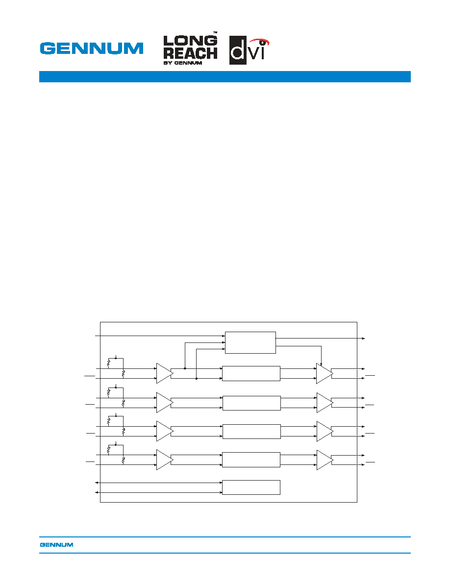
GS8000 Functional Block Diagram
RXC
RXC
RX1
RX1
RX0
RX0
RX2
RX2
TX2
TX2
TX1
TX1
TX0
TX0
TXC
TXC
SCDT
oe
Signal Monitor
& Control
DDC_SDA
DDC_SCL
OE
LONG REACH
TM
TMDS
LONG REACH
TM
DDC
LONG REACH
TM
TMDS
LONG REACH
TM
TMDS
LONG REACH
TM
TMDS

GS8000 Data Sheet
Proprietary and Confidential
25544 - 3
May 2005
2 of 16
Contents
Key Features.................................................................................................................1
Applications...................................................................................................................1
Description ....................................................................................................................1
1. Pin Out ......................................................................................................................3
1.1 Pin Assignment ...............................................................................................3
1.2 Pin Descriptions ..............................................................................................3
2. Electrical Characteristics...........................................................................................5
2.1 DC Electrical Characteristics ..........................................................................5
2.2 AC Electrical Characteristics ...........................................................................7
3. Detailed Description ..................................................................................................9
3.1 Differential Inputs ............................................................................................9
3.2 LONG REACHTM DVI / HDMI .........................................................................9
3.2.1 LONG REACHTM TMDS ........................................................................9
3.2.2 LONG REACHTM DDC...........................................................................9
3.3 Differential Outputs .......................................................................................10
3.4 Signal Monitoring and Control .......................................................................10
3.4.1 Sync Detect Output..............................................................................10
3.4.2 Output Enable......................................................................................10
3.5 System Considerations .................................................................................11
3.5.1 Device Power Up .................................................................................11
3.5.2 ESD Protection ....................................................................................11
3.5.3 Cable Use ............................................................................................11
3.5.4 Complete LONG REACHTM Receive Solution .....................................12
4. Application Reference Design.................................................................................13
4.1 Typical Application Circuit .............................................................................13
4.2 ESD Diodes ..................................................................................................14
4.3 PCB Layout ...................................................................................................14
5. References..............................................................................................................14
6. Package & Ordering Information.............................................................................15
6.1 Package Dimensions ....................................................................................15
6.2 Ordering Information .....................................................................................15
7. Revision History ......................................................................................................16

GS8000 Data Sheet
Proprietary and Confidential
25544 - 3
May 2005
3 of 16
1. Pin Out
1.1 Pin Assignment
1.2 Pin Descriptions
GS8000
(Top View)
VDD
GNDQ
A_VDD
TX2
GNDQ
TX0
VDDQ
VDDQ
TX1
TXC
VDDQ
TXC
TX0
TX1
EXT_RES
GND
VDD
RXC
RX2
GND
RX1
GND
GND
VDD
RX0
VDD
RX2
RX1
RX0
1
34
23
12
RXC
SCDT
D_GND
D_VDD
A_GND
OE
OUT_SWING
TX2
GNDQ
NC
NC
DDC_SCL
DDC_SDA
DDC_VDD
DDC_GND
Table 1-1: Pin Descriptions
Pin Number
Name
Timing
Type
Description
1, 2
RX2, RX2
Analog
Input
Transition minimized differential signal (TMDS) data input 2.
3, 4, 11, 12
GND
Analog
Power
Differential input buffer ground connection.
7, 8, 15, 44
VDD
Analog
Power
Power supply for the differential input buffers. Connect to +3.3V DC.
5, 6
RX1, RX1
Analog
Input
Transition minimized differential signal (TMDS) data input 1.
9, 10
RX0, RX0
Analog
Input
Transition minimized differential signal (TMDS) data input 0.
13, 14
RXC, RXC
Analog
Input
Transition minimized differential signal (TMDS) input clock.
16
EXT_RES
Non
Synchronous
Input
Termination for differential inputs.
An external resistor connected from this input to D_GND is used to
set the input termination.
Use 500
to set the input termination to 50.
17
D_GND
Non
Synchronous
Power
Digital core ground connection.

GS8000 Data Sheet
Proprietary and Confidential
25544 - 3
May 2005
4 of 16
18
OE
Non
Synchronous
Input
CONTROL SIGNAL INPUT
Output enable (active HIGH).
When set HIGH, the differential signal outputs will be active.
When set LOW, the differential signal outputs will mute.
19
SCDT
Non
Synchronous
Output
CONTROL SIGNAL OUTPUT
Sync detect (active HIGH).
Will be set HIGH when a valid signal has been detected at the
RXC/RXC pins.
NOTE: The SCDT pin can be connected to the OE pin to enable an
auto mute upon link inactivity function.
20
D_VDD
Non
Synchronous
Power
Digital core power supply. Connect to +3.3V DC.
21, 22
TXC, TXC
Analog
Output
Transition minimized differential signal (TMDS) output clock.
23, 30, 31
VDDQ
Analog
Power
Power supply for the differential output cable drivers. Connect to
+3.3V DC.
24, 25
TX0, TX0
Analog
Output
Transition minimized differential signal (TMDS) data output 0.
26, 27, 34
GNDQ
Analog
Power
Differential output cable driver ground connection.
28, 29
TX1, TX1
Analog
Output
Transition minimized differential signal (TMDS) data output 1.
32, 33
TX2, TX2
Analog
Output
Transition minimized differential signal (TMDS) data output 2.
35
OUT_SWI
NG
Analog
Input
Differential output signal amplitude.
An external 1% resistor connected from this input to GNDQ is used
to set the differential output signal amplitude.
Use 2k
to set the differential output signal swing to 1V.
36, 37
NC
≠
≠
No connection - leave floating.
38
DDC_GND
Analog
Power
LONG REACHTM DDC ground connection.
39
DDC_VDD
Analog
Power
LONG REACHTM
DDC power supply. Connect to +5V DC.
40
DDC_SCL
Non
Synchronous
I/O
Connect to display data channel (DDC) buffered serial clock (SCL).
41
DDC_SDA
Non
Synchronous
I/O
Connect to display data channel (DDC) buffered serial data (SDA).
42
A_GND
Analog
Power
Analog GND connection.
43
A_VDD
Analog
Power
Analog power supply. Connect to +3.3V DC.
Table 1-1: Pin Descriptions (Continued)
Pin Number
Name
Timing
Type
Description

GS8000 Data Sheet
Proprietary and Confidential
25544 - 3
May 2005
5 of 16
2. Electrical Characteristics
2.1 DC Electrical Characteristics
Table 2-1: Absolute Maximum Ratings
Parameter
Value
Supply Voltage
-0.3V to +3.6V
Input Voltage Range (any input)
-2.0V to +5.25V
Operating Temperature Range
-20∞C to 85∞C
Storage Temperature Range
-50∞C to 125∞C
Lead Temperature (soldering 10 sec.)
260∞C
Table 2-2: DC Electrical Characteristics
VDD = 3.0V to 3.3V, T
A
= 0∞C to 70∞C, unless otherwise shown
Parameter
Symbol
Conditions
Min
Typ
Max
Units
Test
Level
Notes
System
Operating Temperature Range
T
A
≠
0
25
70
∞C
≠
1
-20
≠
85
∞C
≠
2
Supply Voltage
VDD
≠
3.0
3.3
3.6
V
1
1
Supply Voltage for
LONG REACHTM DDC
DDC_VDD
≠
4.75
5.0
5.25
V
1
1
Supply Current
I
D
V
DD
= 3.3V, T
A
= 25∞C
O/P Swing = 1000mV
≠
157
≠
mA
1
≠
Supply Current for
LONG REACHTM DDC
≠
DDC_VDD = 5V
≠
≠
15
mA
1
≠
System Power
P
D
V
DD
= 3.3V, T
A
= 25∞C
O/P Swing = 1000mV
≠
519
≠
mW
5
≠
ESD Protection
≠
All pins
2
≠
≠
kV
≠
3