 | –≠–ª–µ–∫—Ç—Ä–æ–Ω–Ω—ã–π –∫–æ–º–ø–æ–Ω–µ–Ω—Ç: GS9000 | –°–∫–∞—á–∞—Ç—å:  PDF PDF  ZIP ZIP |

DATA SHEET
GENLINX
TM
GS9000C
Serial Digital Decoder
FUNCTIONAL BLOCK DIAGRAM
DEVICE DESCRIPTION
The GS9000C is a CMOS integrated circuit specifically
designed to deserialize SMPTE 259M serial digital signals
at data rates to 370Mb/s.
The device incorporates a descrambler, serial to parallel
convertor, sync processing unit, sync warning unit and
automatic standards select circuitry.
Differential pseudo-ECL inputs for both serial clock and
data are internally level shifted to CMOS levels. Digital
outputs such as parallel data, parallel clock, HSYNC,
Sync Warning and Standard Select are all TTL compatible.
The GS9000C is designed to directly interface with the
GS9005A Reclocking Receiver to form a complete
SMPTE-serial-in to CMOS level parallel-out deserializer.
The GS9000C may also be used with the GS9010A and
the GS9005A to form an adjustment-free receiving system
which automatically adapts to all serial digital data rates.
The GS9015A can replace the GS9005A in GS9000C
applications where cable equalization is not required.
The GS9000C is packaged in a 28 pin PLCC and operates
from a single 5 volt,
±
5% power supply.
FEATURES
∑ fully compatible with SMPTE 259M
∑
decodes 8 and 10 bit serial digital signals for data
rates to 370Mb/s
∑ pin and function compatible with GS9000S, GS9000
and GS9000B
∑ 325mW power dissipation at 270MHz clock rates
∑ incorporates an automatic standards selection
function with the GS9005A Receiver or GS9015A
Reclocker
∑ operates from single +5 or -5 volt supply
∑ enables an adjustment-free Deserializer system
when used with GS9010A and GS9005A or
GS9015A
∑ 28 pin PLCC packaging
APPLICATIONS
∑
4
SC
, 4:2:2 and 360Mb/s serial digital interfaces
∑
Automatic standards select controller for serial routing
and distribution applications using GS9005A Receiver or
GS9015A Reclocker
Revision Date: February 2000
Document No. 522 - 49 - 01
GENNUM CORPORATION P.O. Box 489, Stn. A, Burlington, Ontario, Canada L7R 3Y3
Tel. +1 (905) 632-2996 Fax. +1 (905) 632-5946 E-mail: info@gennum.com
www.gennum.com
GS9000C
SERIAL DATA IN
SERIAL DATA IN
SERIAL CLOCK IN
SERIAL CLOCK IN
LEVEL
SHIFT
SP
SYNC CORRECTION
ENABLE
STANDARDS SELECT
CONTROL
SYNC WARNING
CONTROL
DESCRAMBLER
LEVEL
SHIFT
OSC
2 BIT
COUNTER
PARALLEL
TIMING
GENERATOR
PARALLEL CLOCK
OUT
PARALLEL DATA
OUT (10 BITS)
Sync
Word
Boundary
Sync Error
Hsync Reset
15
11
8
7
6
5
14
SCLK
HSYNC OUTPUT
SS0
SS1
SYNC WARNING
FLAG
30 - BIT
SHIFT REG
SYNC DETECT
(3FF 000 000 HEX)
SYNC CORRECTION
SYNC WARNING
(Schmitt Trigger
Comparator)
AUTO STANDARD SELECT
GS9000C

2
522 - 49 - 01
GS9000C
V
DD
= 5V, T
A
= 0
∞
C to 70
∞
C unless otherwise shown
GS9000C DECODER - DC ELECTRICAL CHARACTERISTICS
V
DD
= 5V, T
A
= 0
∞
C to 70
∞
C unless otherwise shown
GS9000C DECODER - AC ELECTRICAL CHARACTERISTICS
Test Level Legend
1. Production test at room temperature and nominal supply voltage with guardbands for supply and temperature ranges.
2. Production test at room temperature and nominal supply voltage with guardbands for supply and temperature ranges using correlated test.
3. Production test at room temperature and nominal supply voltage.
4. QA sample test.
5. Calculated result based on Level 1, 2, or 3.
6. Not tested. Guaranteed by design simulations.
7. Not tested. Based on characterization of nominal parts.
8. Not tested. Based on existing design/characterization data
of similar product.
R
E
T
E
M
A
R
A
P
L
O
B
M
Y
S
S
N
O
I
T
I
D
N
O
C
N
I
M
P
Y
T
X
A
M
S
T
I
N
U
S
E
T
O
N
T
S
E
T
L
E
V
E
L
y
c
n
e
u
q
e
r
F
k
c
o
l
C
t
u
p
n
I
l
a
i
r
e
S
I
C
S
0
0
1
0
7
3
z
H
M
1
e
t
a
R
a
t
a
D
t
u
p
n
I
l
a
i
r
e
S
R
D
I
D
S
0
0
1
0
7
3
s
/
b
M
1
:
s
t
u
p
n
I
k
c
o
l
C
d
n
a
a
t
a
D
l
a
i
r
e
S
e
m
i
t
e
s
i
R
p
u
t
e
S
d
l
o
H
t
R
t
U
S
t
D
L
O
H
T
A
C
∞
5
2
=
-
0
.
1
0
.
1
0
0
6
-
-
-
-
-
s
p
s
n
s
n
7
7
7
r
e
t
t
i
J
:
k
c
o
l
C
l
e
l
l
a
r
a
P
t
K
L
C
J
T
A
C
∞
5
2
=
-
0
.
1
-
p
-
p
s
n
7
d
n
a
e
m
i
t
e
s
i
R
:
a
t
a
D
l
e
l
l
a
r
a
P
e
m
i
t
l
l
a
F
t
D
P
-
R
n
T
A
,
C
∞
5
2
=
C
L
F
p
0
1
=
-
3
-
s
n
o
t
%
0
2
%
0
8
7
e
c
n
a
r
e
l
o
T
y
a
l
e
D
K
L
C
P
o
t
n
D
P
t
D
-
-
3
±
s
n
g
n
i
s
i
R
f
o
e
g
d
e
t
i
b
o
t
K
L
C
P
d
o
i
r
e
p
e
r
t
n
e
c
7
R
E
T
E
M
A
R
A
P
L
O
B
M
Y
S
S
N
O
I
T
I
D
N
O
C
N
I
M
P
Y
T
X
A
M
S
T
I
N
U
S
E
T
O
N
T
S
E
T
L
E
V
E
L
e
g
a
t
l
o
V
y
l
p
p
u
S
V
S
e
g
n
a
R
g
n
i
t
a
r
e
p
O
5
7
.
4
0
0
.
5
5
2
.
5
V
1
n
o
i
t
p
m
u
s
n
o
C
r
e
w
o
P
)
d
e
d
a
o
l
n
u
s
t
u
p
t
u
o
(
P
C
z
H
M
3
4
1
=
z
H
M
0
7
2
=
z
H
M
0
6
3
=
-
-
-
5
3
2
5
2
3
5
8
3
-
-
-
W
m
W
m
W
m
7
7
1
e
g
a
t
l
o
V
t
u
p
n
I
S
O
M
C
H
I
V
N
I
M
L
I
V
X
A
M
T
A
C
∞
5
2
=
4
.
3
-
-
-
-
5
.
1
V
V
1
1
e
g
a
t
l
o
V
t
u
p
t
u
O
H
O
V
N
I
M
H
O
V
X
A
M
I
H
O
C
∞
5
2
,
A
m
4
=
I
L
O
C
∞
5
2
,
A
m
4
=
4
.
2
-
5
.
4
2
.
0
-
5
.
0
V
V
1
1
t
n
e
r
r
u
C
e
g
a
k
a
e
L
t
u
p
n
I
I
N
I
V
N
I
V
=
D
D
V
r
o
S
S
-
-
0
1
±
A
µ
1
s
t
u
p
n
I
a
t
a
D
d
n
a
k
c
o
l
C
l
a
i
r
e
S
g
n
i
w
S
l
a
n
g
i
S
t
e
s
f
f
O
l
a
n
g
i
S
V
N
I
V
S
O
N
I
T
A
C
∞
5
2
=
T
A
,
C
∞
5
2
=
V
N
I
p
-
p
V
m
0
0
0
1
o
t
0
0
7
=
0
0
7
0
.
3
0
0
8
-
0
0
0
1
0
.
4
p
-
p
V
m
V
f
o
e
r
t
n
e
C
g
n
i
w
s
1
1
ABSOLUTE MAXIMUM RATINGS
PARAMETER
VALUE
Supply Voltage (V
S
= V
DD
- V
SS
)
7V
Input Voltage Range (any input)
-0.3 to (V
DD
+ 0.3)V
DC Input Current (any one input)
±
10
µ
A
Operating Temperature Range
0
∞
C to 70
∞
C
Storage Temperature Range
-65
∞
C to +150
∞
C
Lead Temperature (Soldering, 10 seconds)
260
∞
C
PART NUMBER
PACKAGE TEMPERATURE
GS9000CCPJ
28 Pin PLCC
0
∞
C to 70
∞
C
GS9000CCTJ
28 Pin PLCC Tape
0
∞
C to 70
∞
C
ORDERING INFORMATION

3
522 - 49 - 01
GS9000C
PD7
PD6
PD5
PD4
PD3
PD2
PD1
SDI
SDI
SCI
SCI
SS1
SS0
SSC
(MSB)
V
SS
SWF V
SS
HSYNC PD9 PD8 V
SS
GS9000C
TOP VIEW
V
DD
V
DD
SCE SWC PCLK PD0 V
DD
(LSB)
25
24
23
22
21
20
19
5
6
7
8
9
10
11
12 13 14 15 16 17 18
4 3 2 28 27 26
GS9000C PIN DESCRIPTIONS
PIN NO.
SYMBOL
TYPE
DESCRIPTION
1
HSYNC
Output
Horizontal Sync Output.
CMOS (TTL compatible) output that toggles for each TRS detected.
2
V
SS
Power Supply.
Most negative power supply connection.
3
SWF
Output
Sync Error Warning Flag.
CMOS (TTL compatible) active high output that indicates the
preselected HSYNC Error Rate (HER). The HER is set with an RC time constant on the
SWC input.
4
V
SS
Power Supply.
Most negative power supply connection.
5,6
SDI/SDI
Inputs
Differential, pseudo-ECL serial data inputs
. ECL voltage levels with offset of 3.0V to 4.0V
for operation up to 370MHz.
See AC Electrical Characteristics Table for details.
7,8
SCI/SCI
Inputs
Differential, pseudo-ECL serial clock inputs.
ECL voltage levels with offset of 3.0V to 4.0V
for operation up to 370MHz.
See AC Electrical Characteristics Table for details.
9,10
SS1/SS0
Output
Standard Select Outputs
. CMOS (TTL compatible) outputs used with the GS9005A Receiver in
order to perform an automatic standards select function. These outputs are generated by a 2
bit internal binary counter which stops cycling when there is no CARRIER present at the
GS9005A Receiver input or when a valid TRS is detected by the GS9000C.
11
SSC
Input
Standards Select Control.
Analog input used to set a time constant for the standards select hunt
period. An external RC sets the time constant. When a GS9005A Receiver is used, the open
collector CARRIER DETECT output also connects to this pin in order to enable or disable the
internal 2 bit binary counter which controls the hunting process.
12
V
DD
Power Supply
. Most positive power supply connection.
13
V
DD
Power Supply.
Most positive power supply connection.
14
SCE
Input
Sync Correction Enable.
Active high CMOS input which enables sync correction by not resetting
the GS9000C's internal parallel timing on the first sync error. If the next incoming sync is in error,
internal parallel timing will be reset. This is to guard against spurious HSYNC errors. When SCE
is low, a valid sync will always reset the GS9000C's parallel timing generator.
Fig. 1 GS9000C Pin Outs, 28 Pin PLCC Package
4
522 - 49 - 01
GS9000C
SCE
V
DD
V
DD
SDI
SCI
BIAS
SDI
SCI
V
DD
V
DD
GS9000C PIN DESCRIPTIONS
PIN NO.
SYMBOL
TYPE
DESCRIPTION
15
SWC
Input
Sync Warning Control
. Analog input used to set the HSYNC Error Rate (HER). This is
accomplished by an external RC time constant connected to this pin.
16
PCLK
Output
Parallel Clock Output.
CMOS (TTL compatible) clock output where the rising edge of the clock is
located at the centre of the parallel data window within a given tolerance. See Fig. 7.
17
PD0
Output
Parallel Data Output - Bit 0 (LSB)
. CMOS (TTL compatible) descrambled parallel data output from
the serial to parallel convertor representing the least significant bit (LSB).
18
V
DD
Power Supply
. Most positive power supply connection.
19 - 25
PD1 - PD7
Outputs
Parallel Data Outputs - Bit 1 to Bit 7.
CMOS (TTL compatible) descrambled parallel data outputs from
the serial to parallel convertor representing data bit 1 through data bit 7.
26
V
SS
Power Supply.
Most negative power supply connection.
27
PD8
Output
Parallel Data Output.
CMOS (TTL compatible) descrambled parallel data output from the serial to
parallel convertor representing data bit 8.
28
PD9
Output
Parallel Data Output - Bit 9 (MSB).
CMOS (TTL compatible) descrambled data output from the serial
to parallel convertor representing the most significant bit (MSB).
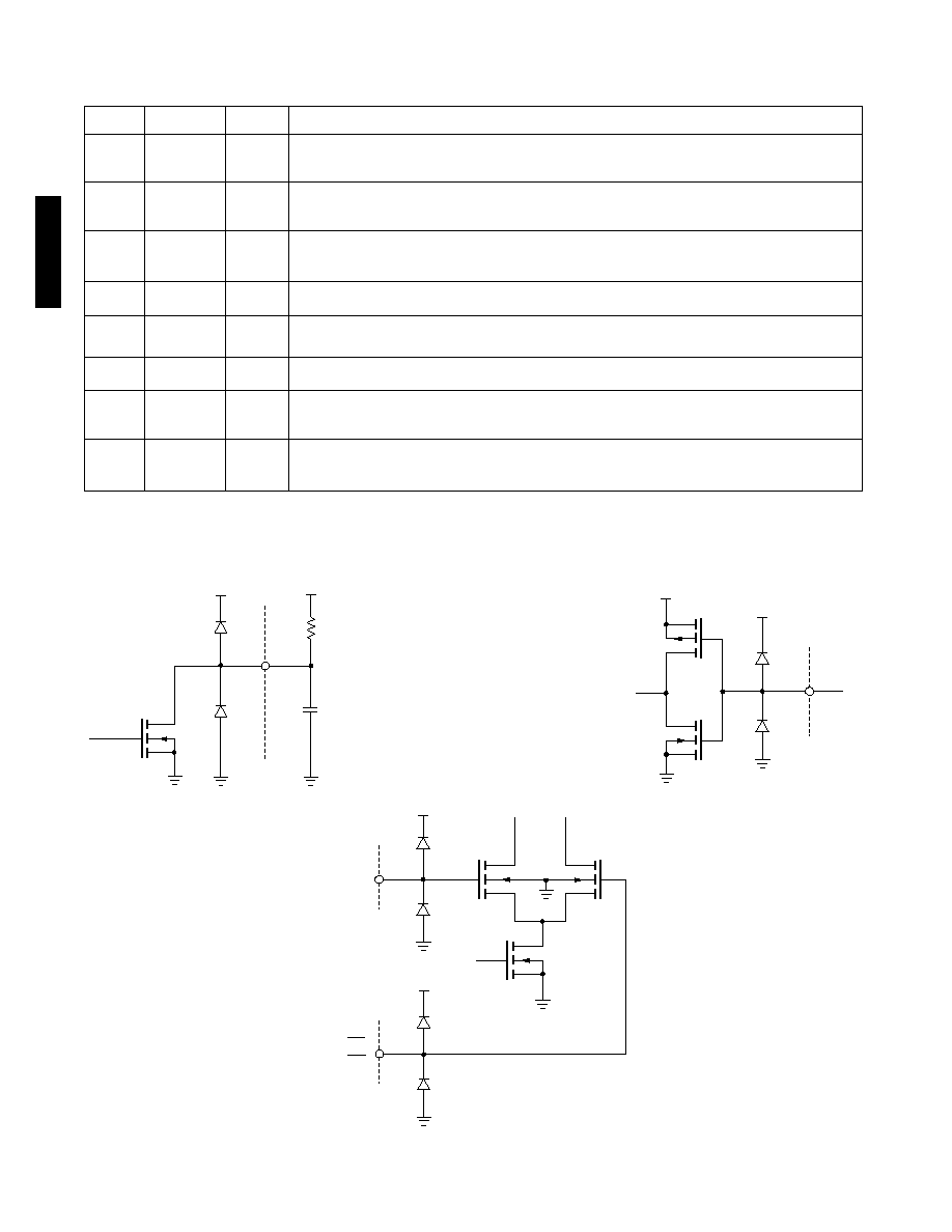
INPUT / OUTPUT CIRCUITS
Fig. 4 Pins 5 - 8 SDI - SCI
Fig. 2 Pin 11 SSC
Fig. 3 Pin 14 SCE
R
EXT
EXTERNAL
COMPONENTS
SSC
V
DD
V
DD

5
522 - 49 - 01
GS9000C
R
EXT
C
EXT
SWC
EXTERNAL
COMPONENTS
V
DD
V
DD
6k8
Fig. 5 Pin 15 SWC
Fig. 6 Pins 3, 16, 17, 19 - 25, 27, 28
SWF, HSYNC, SSI, SSD, PCLK, PD0-9
Fig. 7 Waveforms
In order to maintain very short interconnections when
interfacing with the GS9005A Receiver, the critical high
speed inputs such as Serial Data (pins 5 and 6) and Serial
Clock (pins 7 and 8) are located along one side of the device
package.
If the automatic standard select function is not used, the
Standard Select bits (pins 9 and 10) do not need to be
connected, however the control input (pin 11) should be
grounded.
TEST SET-UP & APPLICATION INFORMATION
Figure 8 shows the test set-up for the GS9000C operating
from a V
DD
supply of +5 volts. The differential pseudo ECL
inputs for DATA and CLOCK (pins 5,6,7 and 8) must be
biased between +3.0 and +4.0 volts. In the circuit shown,
these inputs with the resistor values shown, can be directly
driven from the outputs of the GS9005A Reclocking Receiver.
In other cases, such as true ECL level driver outputs, two
biasing resistors are needed on the DATA and CLOCK inputs
and the signals must be AC coupled.
It is critical that the decoupling capacitors connected to pins
12,13 and 18 be chip types and be located as close as
possible to the device pins.
GND
OUTPUT
V
DD
t
SU
t
HOLD
t
CLKL
=
t
CLKH
SERIAL
CLOCK
(SCI)
SERIAL
DATA
(SDI)
50%
PARALLEL
DATA
(PDn)
50%
PARALLEL
CLOCK
(PCLK)
1/
2
T
1/
2
T
t
D

6
522 - 49 - 01
GS9000C
DECODER
GS9000C
1
4
3
6
5
7
SDI
SDI
SCI
SCI
SS1
SS0
SSC
9
8
10
2
PARALLEL DATA BIT 0
PARALLEL DATA BIT 1
PARALLEL DATA BIT 2
PARALLEL DATA BIT 3
PARALLEL DATA BIT 4
PARALLEL DATA BIT 5
PARALLEL DATA BIT 6
PARALLEL DATA BIT 7
PARALLEL DATA BIT 8
PARALLEL DATA BIT 9
PARALLEL CLOCK OUT
SYNC CORRECTION ENABLE
HSYNC OUTPUT
STANDARDS SELECT BIT 1
STANDARDS SELECT BIT 0
3 x 100n
**
17
18
19
20
15
16
14
12
13
11
+5V
PD0
PDI
PD2
PD3
PD4
PD5
PD6
PD7
PD8
PD9
PCLK
SCE
V
SS
V
SS
V
SS
SWC SWF
V
DD
V
DD
V
DD
HSYNC
21
22
23
24
25
27
28
26
10p
+5V
** Locate the three 0.10
µ
F decoupling
capacitors as close as possible to the
corresponding pins on the GS9000C.
Chip capacitors are recommended.
SYNC WARNING FLAG
SDI
IN
SDI
IN
SCI
IN
SCI
IN
39k
13 x 425
+5V
100k
820p
22
µ
All resistors in ohms,
all capacitors in farads,
unless otherwise specified.
Fig. 8 GS9000C Test Set-Up
With correctly synchronized serial data and clock connected
to the GS9000C, the HSYNC output (pin 1) will toggle for each
HSYNC detected. The Parallel Data bits PD0 through PD9
along with the Parallel Clock can be observed on an
oscilloscope or fed to a logic analyzer. These outputs can
also be fed through a suitable TTL to ECL converter to directly
drive parallel inputs to receiving equipment such as monitors
or digital to analog converters.
In operation, the HSYNC output from the GS9000C decoder
toggles on each occurrence of the timing reference signal
(TRS). The state of the HSYNC output is not significant, just
the time at which it toggles.
The HSYNC output toggles to indicate the presence of the
TRS on the falling edge of PCLK, one data symbol prior to the
output of the first word in the TRS. In the following diagram,
data is indicated in 10 bit Hex.
T
R
S
T
R
S
T
R
S
ACTIVE VIDEO
& H BLANKING
ACTIVE VIDEO
& H BLANKING
E
A
V
H
BLNK
S
A
V
ACTIVE
VIDEO
E
A
V
H
BLNK
S
A
V
4
SC
DATA
STREAM
HSYNC
OUT
4:2:2
DATA
STREAM
HSYNC
OUT
Fig. 9 Operation of HSYNC Output
XXX 3FF 000 000 XXX
XXX 3FF 000 000 XXX
PCLK
PDN
HSYNC
Fig. 10 Operation of HSYNC with Respect to PCLK

7
522 - 49 - 01
GS9000C
Figure 11 shows an application of the GS9000C in an
adjustment free, multi-standard serial to parallel convertor.
This circuit uses the GS9010A Automatic Tuning Sub-system
IC and a GS9005A Serial Digital Receiver. The GS9005A may
be replaced with a GS9015A Reclocker IC if cable equalization
is not required.
The GS9010A ATS eliminates the need to manually set or
externally temperature compensate the Receiver or Reclocker
VCO. The GS9010A can also determine whether the incoming
data stream is 4sc NTSC,4sc PAL or component 4:2:2.
The GS9010A includes a ramp generator/oscillator which
repeatedly sweeps the Receiver/Reclocker VCO frequency
over a set range until the system is correctly locked. An
automatic fine tuning (AFT) loop maintains the VCO control
voltage at its centre point through continuous, long term
adjustments of the VCO centre frequency.
During normal operation, the GS9000C Decoder provides
continuous HSYNC pulses which disable the ramp/oscillator
of the GS9010A. This maintains the correct Receiver/
Reclocker VCO frequency. When an interruption to the incoming
data stream is detected by the Receiver/Reclocker, the
Carrier Detect goes LOW and tri-states the AFT loop in order
to maintain the correct VCO frequency for a period of about
2 seconds. This allows the Receiver/Reclocker to rapidly
relock when the signal is re-established.
GS9000C, GS9005A and GS9010A INTERCONNECTIONS
Fig. 11 Application Circuit - Adjustment Free Multi-standard Serial to Parallel Convertor
STANDARD TRUTH TABLE
/2 P/N STANDARD
0 0 4:2:2 - 270
0 1 4:2:2 - 360
1 0 4sc - NTSC
1 1 4sc - PAL
P/N
OUT
IN-
COMP
LF
/2
V
CC
SWF
1
2
3
4
5
6
7
8
16
15
14
13
12
11
10
9
PARALLEL DATA BIT 9
PARALLEL DATA BIT 8
PARALLEL DATA BIT 7
PARALLEL DATA BIT 6
PARALLEL DATA BIT 5
PARALLEL DATA BIT 4
PARALLEL DATA BIT 3
PARALLEL DATA BIT 2
PARALLEL DATA BIT 1
PARALLEL DATA BIT 0
PARALLEL CLOCK OUT
SYNC CORRECTION ENABLE
HSYNC OUTPUT
SYNC WARNING FLAG
INPUT SELECTION
STDT
V
CC
CD
HSYNC
GND
OSC
DLY
FVCAP
10
µ
10
µ
10
µ
+
+
+
V
CC
+5V
+5V
V
CC
V
CC
V
CC
0
µ
1
100
100
100
100
390
390
390
390
0
µ
1
0
µ
1
0
µ
1
25
24
23
22
21
20
19
5
6
7
8
9
10
11
4 3 2 1 28 27 26
12 13 14 15 16 17 18
910
22n
(1)
(2)
(2)
(2)
(3)
75
113
75
47p
5p6
10n
0
µ
1
0
µ
1
3n3
82n
180n
0
µ
68
0
µ
1
22n
DGND
DGND
DGND
DGND
47p
0
µ
1
DGND
GND
1k2
1k2
68k
100 100
120
50k
0.1
µ
100k
SWF
GS9010A
INPUT
ECL
DATA
INPUT
DDI
DDI
V
CC2
SDI
SDI
/2
V
EE3
SDO
SDO
SCO
SCO
SS1
SS0
CD
V
CC
1
V
EE1
AGC
A/D
SSI
V
EE2
V
CC4
LOOP
R
VCO0
R
VCO1
R
VCO2
EYE
OUT
R
VCO3
V
CC3
25
24
23
22
21
20
19
5
6
7
8
9
10
11
4 3 2 1 28 27 26
0
µ
1
DGND
DGND
SSI
100
100
100
3k3
100
100
100
100
100
100
100
GS9000C
SDI
SDI
SCI
SCI
SS1
SS0
SSC
PD7
PD6
PD5
PD4
PD3
PD2
PD1
V
SS
SWF
V
SS
HSYNC
PD9
PD8
V
SS
V
DD
V
DD
SCE
SWC
PCLK
PDO
V
DD
STAR
ROUTED
12 13 14 15 16 17 18
V
CC
V
CC
V
CC
V
CC
6
µ
8
6
µ
8
+
+
GS9005A
V
CC
V
CC
DV
CC
DV
CC
DV
CC
V
CC
DV
CC
V
CC
SWF
(1) Typical value for input return loss matching
(2) To reduce board space, the two anti-series 6.8
µ
F capacitors (connected across pins 2 and 3 of the GS9010A)
may be replaced with a 1.0
µ
F non-polarized capacitor provided that
(a) the 0.68
µ
F capacitor connected to the OSC pin (11) of the GS9010A is replaced with a 0.33
µ
F capacitor and
(b) the GS9005A /15A Loop Filter Capacitor is 10nF.
(3) Remove this potentiometer if P/N function is not required, and ground pin 16 of the GS9010A.

8
522 - 49 - 01
GS9000C
SYNC WARNING FLAG OPERATION
Fig. 10 Sync Warning Flag Circuit
Each time HSYNC is not correctly detected, the Sync Warning
Flag output (pin 3 ) will go HIGH. The RC network connected
to the Sync Warning Control input (pin 15) sets the number
of sync errors that will cause the SWF pin to go HIGH. The
component values of the RC network shown in Figure 10 set
the SWF error rate to approximately one HSYNC error in 10
lines. These component values are chosen for optimum
performance of the SWF pin, and should not be adjusted.
Typically, HSYNC errors will become visible on a monitor
before the SWF will provide an indication of HSYNC errors.
As a result, the SWF function can be used in applications
where the detection of significant signal degradation is
desired.
A high SWF will go low as soon as the input error rate
decreases below the set rate. This response time is
determined by C, as mentioned earlier. A small amount of
hysteris in the comparator ensures noise immunity.
Gennum Corporation assumes no responsibility for the use of any circuits described herein and makes no representations that they are free from patent infringement.
© Copyright August 1999 Gennum Corporation. All rights reserved. Printed in Canada.
DOCUMENT IDENTIFICATION:
DATA SHEET
The product is in production. Gennum reserves the right to make changes
at any time to improve reliability, function or design, in order to provide
the best product possible.
CAUTION
ELECTROSTATIC
SENSITIVE DEVICES
DO NOT OPEN PACKAGES OR HANDLE
EXCEPT AT A STATIC-FREE WORKSTATION
GENNUM CORPORATION
MAILING ADDRESS:
P.O. Box 489, Stn. A, Burlington, Ontario, Canada L7R 3Y3
Tel. +1 (905) 632-2996 Fax +1 (905) 632-2814
SHIPPING ADDRESS:
970 Fraser Drive, Burlington, Ontario, Canada L7L 5P5
GENNUM JAPAN CORPORATION
C-101, Miyamae Village, 2-10-42 Miyamae, Suginami-ku, Tokyo 168-0081, Japan
Tel. +81 (3) 3334-7700 Fax: +81 (3) 3247-8839
GENNUM UK LIMITED
25 Long Garden Walk, Farnham, Surrey, England GU9 7HX
Tel. +44 (0) 1252 747000 Fax +44 (0) 1252 726523
SYNC
WARNING
FLAG
(SWF)
3
6k8
V
DD
V
DD
15
SYNC
ERROR
COMPARATOR
SYNC
WARNING
CONTROL
-
+
REVISION NOTES
Updated values in Electrical Characteristics tables and added test levels
with legend; Updated Figure 8 (Test Set-Up); Changed document from
preliminary data sheet to data sheet; Standardized artwork.
For the latest product information, visit www.gennum.com.