 | –≠–ª–µ–∫—Ç—Ä–æ–Ω–Ω—ã–π –∫–æ–º–ø–æ–Ω–µ–Ω—Ç: GS9010A | –°–∫–∞—á–∞—Ç—å:  PDF PDF  ZIP ZIP |
STANDARDS
THRESHOLD ADJUST
OUT
(to GS9005A)
IN-
2
1
13
3
HSYNC
( (from GS9000B
o orGS9000S)
V
REF
20k
25k
18k
+
-
+
-
OSCILLATOR
COMPOSITE /
COMPONENT
DETECTOR
˜
4
4
5
14
11
6
10
9
8
16
PAL/NTSC
FREQUENCY
COMPENSATION
LOOP FILTER
(from GS9005A)
OSCILLATOR
/2
(to GS9005A)
DELAY
CARRIER DETECT
(from GS9005A)
FV CAP
SWF
(from GS9000B
or GS9000S)
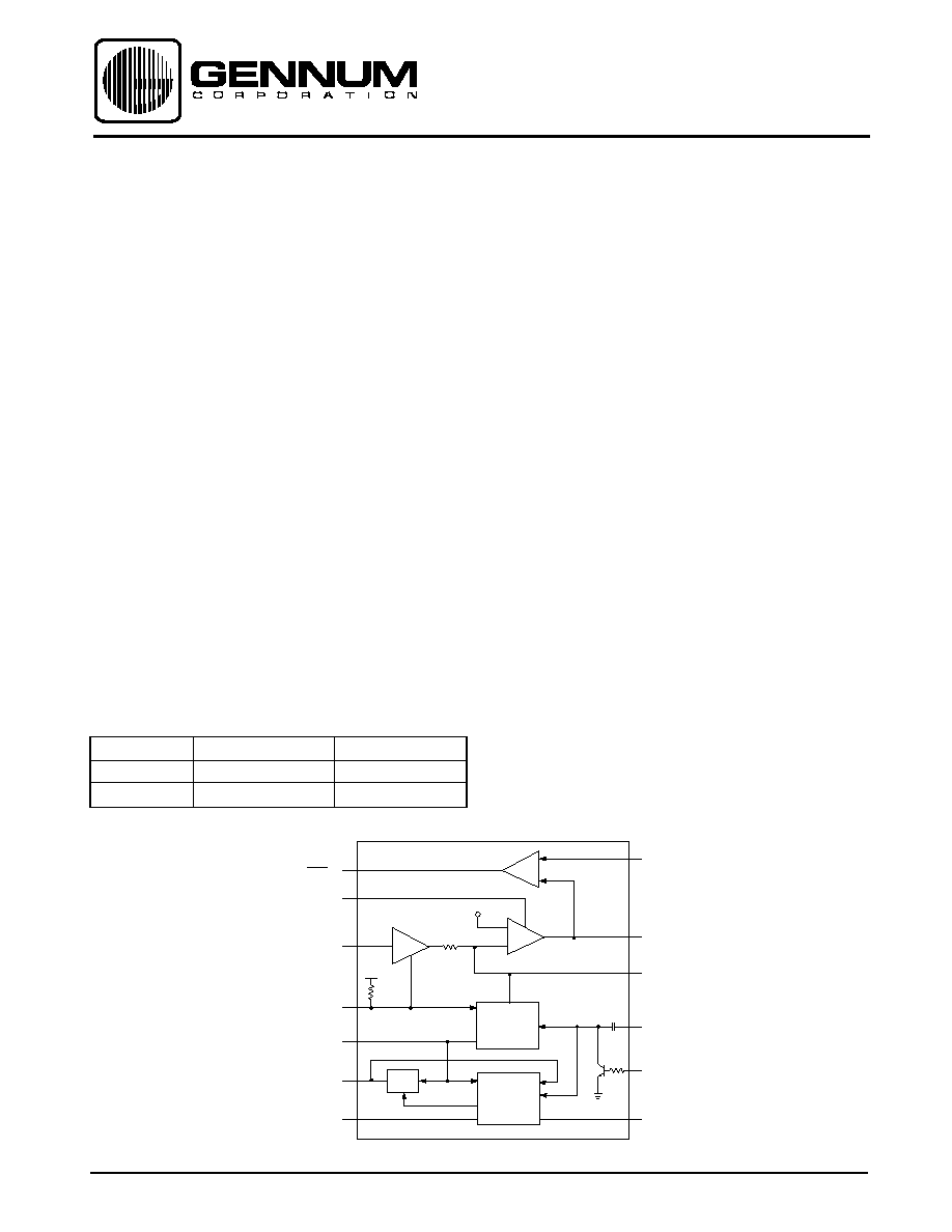
DEVICE DESCRIPTION
The
GENLINX
TM
GS9010A is a monolithic integrated
circuit designed to be an Automatic Tuning Subsystem
(ATS) when used with the GS9005A Receiver or the
GS9015A Reclocker and the GS9000B or GS9000S Decoder.
The GS9010A ATS eliminates the need to manually set or
externally temperature compensate the Receiver or Reclocker
VCO. The GS9010A can also determine whether the
incoming data stream is 4sc NTSC, 4sc PAL or component
4:2:2.
The GS9010A is an enhanced version of the GS9010. Pin
compatible with the GS9010, the GS9010A offers improved
noise immunity to spurious HSYNC signals.
The GS9010A includes a ramp generator/oscillator which
repeatedly sweeps the Receiver/Reclocker VCO
frequency
over a set range until the system is correctly locked. Once
locked, an automatic fine tuning (AFT) loop maintains the
VCO control voltage at its optimum centre point over
variations in temperature. During normal operation, the
GS9000B or GS9000S Decoder provides continuous HSYNC
pulses which disable the ramp/oscillator of the GS9010A.
This maintains the correct Receiver/Reclocker VCO
frequency. When an interruption to the incoming data
stream is detected by the Receiver/Reclocker, the Carrier
Detect goes LOW and opens the AFT loop in order to
maintain the correct VCO frequency for a period of typically
2 seconds. If the signal is re-established within this 2
seconds, the Receiver/Reclocker will rapidly relock. For
periods longer than typically 2 seconds, the VCO slowly
drifts towards a minimum frequency. Typically after 2
minutes, the serial clock output of the PLL settles to
approximately 85 MHz when /2 is high or 170 MHz
when /2 is low. The GS9010A is packaged in a 16 pin
wide SOIC, operates from a single +5 or -5 volt supply
and typically consumes 40 mW of power.
FEATURES
∑
when used with the GS9005A or GS9015A and the
GS9000B or GS9000S, the GS9010A:
- constitutes an automatic 'tweakless' Serial
Digital receiving system
- eliminates the need for trim pots and external
temperature compensation for bit rates to 370 Mb/s
- automatically determines whether data is 4sc
or 4:2:2, and whether the 4sc data is NTSC or
PAL
- acquires lock from a 'no signal' condition in typically
50 ms
- holds lock during data interruptions for typically 2s
- relocks from synchronous switching in less than
10
µ
s
∑
16 pin SOIC packaging
∑
operates from a single +5 or -5 volt supply
∑
typically consumes only 40 mW
∑
immunity to spurious HSYNC inputs
∑
defines minimum GS9005A VCO frequency after
extended absence of input signal
∑
matches GS9005A capture range
DATA SHEET
GENLINX
TM
GS9010A Serial Digital
Automatic Tuning Subsystem
Revision Date: August 1997
FUNCTIONAL BLOCK DIAGRAM
APPLICATIONS
∑ 4sc, 4:2:2 & 360 Mb/s serial digital interfaces
ORDERING INFORMATION
Part Number Package Type Temperature Range
GS9010ACKC 16 Pin Wide SOIC 0
∞
to 70
∞
C
GS9010ACTC 16 Pin Wide SOIC Tape 0
∞
to 70
∞
C
GENNUM CORPORATION P.O. Box 489, Stn A, Burlington, Ontario, Canada L7R 3Y3 tel. (905) 632-2996 fax: (905) 632-5946
Gennum Japan Corporation: A-302 Miyamae Village, 2-10-42 Miyamae, Suginami-ku, Tokyo 168, Japan tel. (03) 3334-7700 fax (03) 3247-8839
Document No. 521 - 01 - 05
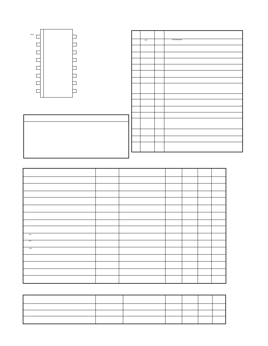
2
521 - 01 - 05
1
P/N
O
PAL/NTSC Output
2
OUT
O
Output to Receiver/Reclocker R
VCO
resistor
3
IN-
I
Inverting input to internal amplifier
4
COMP
I
Frequency compensating Capacitor
5
LF
I
Loop Filter input from Receiver/Reclocker
6
/2
O
Divide by two output to Receiver/Reclocker
7
V
CC
Most positive supply voltage
8
SWF
I
Sync Warning Flag Input from GS9000B
or GS9000S
9
FV CAP
I
Capacitor for frequency to voltage converter
10
DLY
I
Capacitor for internal delay
11
OSC
I
RC time constant for internal oscillator
12
GND
Most negative supply voltage
13
HSYNC
I
HSYNC input from GS9000B or GS9000S
Decoder
14
CD
I
Carrier Detect input from Receiver/Reclocker
15
V
CC
Most positive supply voltage
16
STDT
I
Standards threshold adjust input from
external potentiometer
PIN CONNECTIONS
Supply Voltage
V
S
4.75
5.0
5.25
V
Supply Current
I
S
5.5
8.0
10.0
mA
OUT Voltage Maximum
V
OUT MAX
V
LF
= 2.7 V
2.2
2.3
2.4
V
LF Input Bias
I
LF
V
LF
= 2.3 V
-10
0
10
nA
IN Input Bias
I
IN
CD Low
0
5
70
nA
STDT Input Bias
I
STDT
V
STDT
= 1.5 V
-10
-0.5
0
µ
A
STDT Input Voltage
V
STDT
0
-
3
V
CD Input Pull-Up Resistor
RCD
13.5
18
22.5
k
P/N Low-Level Output Voltage
V
P/NL
I
L
= 0
-
-
0.2
V
P/N Low-Level Output Current
I
P/NL
-1
-
-
mA
P/N Output Pull-Up Resistor
-
30
-
k
/2 High-Level Output Voltage
V
/2H
I
L
= 0
4
4.6
-
V
/2 Low-Level Output Voltage
V
/2L
I
L
= 0
-
-
0.2
V
/2 Output Current
I
/2
-
±
40
-
µ
A
SWF Input Bias
I
SWF
V
SWF
= 5 V
150
200
250
µ
A
PARAMETER
SYMBOL CONDITIONS MIN TYP MAX UNITS
HSYNC Input Frequency for /2 High
COMPOSITE
V
CC
= 4.75 to 5.25
-
7.85
11.0
kHz
HSYNC Input Frequency for /2 Low
COMPONENT
V
CC
= 4.75 to 5.25
11.0
15.7
-
kHz
HSYNC Input Rise / Fall Time
tr
HSYNC
CMOS Driving Levels
-
-
100
ns
PARAMETER
SYMBOL CONDITIONS MIN TYP MAX UNITS
( V
CC
= 5 V, T
A
= 0
∞
C to 70
∞
C, unless otherwise specified)
GS9010A DC ELECTRICAL CHARACTERISTICS
GS9010A AC ELECTRICAL CHARACTERISTICS
( V
CC
= 5 V, T
A
= 0
∞
C to 70
∞
C, unless otherwise specified)
ABSOLUTE MAXIMUM RATINGS
Parameter
Value/Units
Supply Voltage
±
5.5 V
Input Voltage Range (any input)
-V
EE
< V
I
< V
CC
DC Input Current (any one input)
10mA
Operating Temperature Range
0
∞
C
T
A
70
∞
C
Storage Temperature Range
-65
∞
C
T
S
150
∞
C
Lead Temperature (soldering, 10 seconds)
260
∞
C
P/N
IN -
COMP
LF
CD
HSYNC
/2
V
CC2
GND
OSC
DLY
STDT
V
CC1
14
9
15
10
12
13
11
GS9010A
OUT
SWF
FV CAP
16
1
4
3
6
5
7
2
8
PIN
No.
SYMBOL TYPE DESCRIPTION
GS9010A PIN DESCRIPTIONS

3
521 - 01 - 05
SYSTEM DESCRIPTION
The GS9005A Receiver or GS9015A Reclocker along with the
GS9000B or GS9000S Decoder form a serial to parallel decoding
system for Serial Digital Video signals. Use of the GS9010A
eliminates the need to manually tune the VCO and externally
temperature compensate for all data rates. Figure 1 shows a
simplified block diagram of the Automatic Tuning Sub-System
and Figure 2 shows the relevant waveforms.
The active high CARRIER DETECT output of the Receiver/
Reclocker indicates the presence of serial data. If the CARRIER
DETECT input to the GS9010A (pin 14) is HIGH (see Fig 2. [A])
and a Timing Reference Signal (TRS) is not being detected by
the GS9000B or GS9000S Decoder, an oscillator in the GS9010A
produces a s a w t o o t h r a m p s i g n a l a t t h e O U T p i n
( p i n 2 ) ( s e e Figure 2. [C]). This output is connected to the
Receiver/Reclocker R
VCO
pin via a resistor which converts this
voltage ramp into a current ramp. The frequency of the VCO is
changed by varying the current drawn from the R
VCO
pin such
that a lower sweep voltage at pin 2 of the GS9010A causes a
higher VCO frequency.
As the frequency sweeps, the PLL will lock to the incoming data
stream and the GS9000B or GS9000S decoder will detect TRS.
The TRS detect function is provided by the HSYNC output of the
GS9000B or GS9000S. In this case, HSYNC is a digital signal
which changes state whenever TRS is detected. This signal is
connected to the HSYNC input (pin 13) of the GS9010A (see
Figure 2 [B]). This signal will be at a rate equal to one half the
horizontal scan rate for composite video and equal to the
horizontal scan rate for component video since both EAV and
SAV produce an HSYNC state change. The presence of
detected TRS will shut off the GS9010A oscillator and disable
the sweep. Even though the oscillator is off, the Automatic Fine
Tuning (AFT) function provided by the buffer amplifier in the
GS9010A remains in the control loop in order to centre the
GS9005A or GS9015A loop filter voltage to V
REF
(approximately
2.3V).
The VCO within the GS9005A or GS9015A has a dual modulus
divider feature which optimises jitter performance for the lower
data rates. This feature is enabled by a logic HIGH on the /2
pin. The MODULUS CONTROL output (pin 6) (see Figure 2.
[D]) of the GS9010A controls this /2 function to set the VCO
frequency to twice the normal rate. Under normal operation the
VCO within the GS9005A or GS9015A, operates at twice the
output clock frequency, which means that for 360 Mb/s data the
VCO is operating at 720 MHz (2 x 360 MHz). For 177 Mb/s (PAL
- 4fsc), with the /2 function enabled, the VCO operates at 708
MHz (2 x 2 x 177 MHz). In the case of component and
composite NTSC, the VCO operates at 540 MHz (2 x 270 MHz)
and 572 MHz (2 x 2 x 143 MHz) respectively. This means that
the VCO is tuned to the same frequency range for 4:2:2 and the
respective 4sc signals.
The MODULUS CONTROL itself is derived by dividing the
GS9010A oscillator by four. It is possible that the PLL could lock
with the MODULUS CONTROL in the wrong state (/2 OFF) for
component data rates.
In order to avoid this, another circuit ensures that the MODULUS
CONTROL is set HIGH (/2 ENABLED) for composite data
rates and LOW (/2 OFF) for component data rates. This is
accomplished through a Frequency Detector (Frequency to
Voltage Convertor, FVC) which measures the frequency of
HSYNC and compares it to a reference. If the frequency of
HSYNC corresponds to composite video, the comparator
output is high and the
˜
4 (MODULUS CONTROL) is set HIGH.
Conversely, when the frequency of HSYNC corresponds to
component video, the MODULUS CONTROL is set LOW.
If the FVC measurement results in any change to the MODULUS
CONTROL, the PLL will immediately lose lock, the TRS will not
be detected and the oscillator will begin to sweep the VCO
frequency. Now the PLL will reacquire lock with the MODULUS
CONTROL in the correct state before the
˜
4 output changes
state.
In a noisy environment or at power-on, erratic TRS will cause
the GS9000B or GS9000S to output an artificially low HSYNC
frequency. This condition often subsides after input data
stabilizes or in the case of power-up, once the supplies have
settled. The GS9010A employs a technique to provide noise
immunity within the COMPOSITE/COMPONENT DETECTOR
(CCD) to protect against erroneous modulus settings. This
technique is explained in the following paragraph.
A delay is required for the FVC calculation within the CCD
before the
˜
4 is set/reset. In the GS9010A, the trigger
threshold for this delay is controlled by the /2 and FVCAP
output voltage. Because this threshold is modulated, the
incoming HSYNC frequency must be compatible with the
current /2 state before the delay is triggered. This threshold
control prevents artificially low HSYNC frequencies from
triggering the set/reset of the
˜
4 thus preventing the wrong
MODULUS CONTROL.
If the serial digital signal is interrupted, CARRIER DETECT
(pin 14) goes LOW and turns the internal oscillator off. The
buffer from the LOOP FILTER input (pin 5) to the 20 k
integrator resistor is disabled and its output becomes high
impedance, neither sinking nor sourcing current. In this state,
the output voltage from the GS9010A will remain constant for
a time period of typically 2 seconds. The VCO in the Receiver/
Reclocker will remain tuned to the correct frequency so that
the PLL will relock quickly without frequency sweeping when
the serial data returns. For longer periods of data interruption,
the external integration capacitor between the OUT and IN
pins will slowly discharge and the VCO will drift lower in
frequency. The serial clock output frequency of the PLL will
settle to approximately 170 MHz when /2 is high and 85 MHz
when /2 is low. A limit has been set on the maximum OUT
voltage to prevent Receiver/Reclocker VCO shutdown allowing
faster relock time once data is reapplied.

4
521 - 01 - 05
PAL/NTSC THRESHOLD ADJUST
To adjust the P/N threshold using a potentiometer, monitor the
OUT voltage at pin 2 of the GS9010A. Start with a composite
NTSC source, and record the voltage at pin 2 as V
NTSC
. Now
connect a PAL source to the input and record the voltage at pin
2 as V
PAL
. Adjust the reference voltage, V
REF
at pin 16 to a value
approximately halfway between V
PAL
and V
NTSC
, i.e. V
REF
=
(V
NTSC
+ V
PAL
)/2. The P/N threshold will now be set.
Gating of the HSYNC input is available on the SWF pin. This
gating is used with the GS9010A to improve immunity to
missing TRS detection during power-up or in noisy system
applications.
Capacitor values for the GS9010A should be used as indicated
in Figure 3. These capacitors have been optimised to
produce correct system operation.
GS9010 REPLACEMENT NOTE:
To ensure proper operation of the GS9010A, the resistor
network connected between the GS9010A OUT (pin 2) and
GS9005A R
VCO3
(pin 17), and the value of FVCAP (pin 9) must
be as per this data sheet (Figure 3). Replacing a GS9010 with
a GS9010A will require modification to these component
values.
RE-TIMED DATA
RECOVERED CLOCK
RVCO
1k2
1k2
100nF
120
THRESHOLD
ADJUST
SERIAL
DATA IN
2
1
13
8
HSYNC
V
REF
C
INT
20k
SWF
+
-
OSCILLATOR
COMPOSITE /
COMPONENT
DETECTOR
PAL/NTSC
˜
4
5
14
LOOP
FILTER
6
16
+5V
MODULUS
CONTROL
/2
CARRIER
DETECT
GS9005A/GS9015A
GS9000B/GS9000S
GS9010A
SERIAL
DIGITAL
PLL
DIGITAL
VIDEO
DECODER
+
-
18k
25k
All resistors in ohms, all capacitors in microfarads unless otherwise stated.
Fig. 1 Automatic Tuning Sub System Block Diagram

5
521 - 01 - 05
(A) CARRIER
DETECT
(PIN 14)
(C) OUT
(PIN 2)
2 SECONDS
2 MINs
(D) /2
(PIN 6)
(B) HSYNC
(PIN 13)
TRS
TRS
LOOP
LOCKED
LOOP
LOCKED
COMPONENT VIDEO
COMPOSITE VIDEO
(NOT TO SCALE)
Fig. 2 System Waveform Diagrams
APPLICATIONS
Figure 3 shows a typical application circuit using the GS9010A
in an autotuning SDI receiver.
Correct operation of an autotuning receiver is determined by
using a suitable EDH measurement tool or Digital to Analog
Monitor to verify error free performance.
The correct operation of a locked autotuning receiver can be
verified by referring to Figure 2. The HSYNC output from the
GS9000B or GS9000S decoder will toggle on each occurrence
of the Timing Reference Signal (TRS). The state of the HSYNC
output is not significant, just the rate at which it toggles.
Application Note - PCB Layout
Special attention must be paid to component layout when
designing high performance serial digital receivers.
For background information on high speed circuit and layout
design concepts, refer to Document No. 521-32-00, "Optimizing
Circuit and Layout Design of the GS90005A/15A". A recom-
mended PCB layout can be found in the Gennum Application
Note "EB9010B Deserializer Evaluation Board"
The use of a star grounding technique is required for the loop
filter components of the GS9005A/15A.
Controlled impedance PCB traces should be used for the
differential clock and data interconnection between the
GS9005A and the GS9000B or GS9000S. These differential
traces must not pass over any ground plane discontinuities. A
slot antenna is formed when a microstrip trace runs across a
break in the ground plane.
The series resistors at the parallel data output of the
GS9000B/S are used to slow down the fast rise/fall time of the
GS9000B/S outputs. These resistors should be placed as
close as possible to the GS9000B or GS9000S output pins to
minimize radiation from these pins.