
GENNUM CORPORATION P.O. Box 489, Stn. A, Burlington, Ontario, Canada L7R 3Y3
Tel. +1 (905) 632-2996 Fax. +1 (905) 632-5946 E-mail: info@gennum.com
www.gennum.com
Revision Date: November 1999
Document No. 521 - 66 - 05
DATA SHEET
G
S
9
020
FEATURES
∑ fully compatible with SMPTE 259M
∑ auto-standard operation to 540MHz
∑ embedded EDH and data processing core
∑ selectable loop through or re-serialized EDH-
processed serial output
∑ noise immune HVF timing signal outputs
∑ configurable FIFO reset pulse for clearing
downstream FIFOs
∑ ANC header and TRS-ID correction for all standards
∑ user controlled output blanking
∑ ITU-R-601 output clipping for active picture area
∑ ancillary data indication
∑ low system power
∑ selectable I≤C interface or 8-bit parallel port for access
to EDH flags and device configuration bits
∑ EDH flags also available on dedicated pins
∑ seamless flag mapping to GS9021 EDH coprocessor
∑ 80 pin LQFP
APPLICATIONS
SMPTE 259M serial digital receiver for composite and
component standards including 4:4:4:4 at 540Mb/s with
EDH processing; Noise immune digital sync and timing
generation; Cost effective EDH insertion and checking for
serial routing and distribution applications.
DESCRIPTION
The GS9020 is specifically designed to deserialize SMPTE
259M serial digital signals. The inclusion of Error Detection
and Handling (EDH) ensures the integrity of the data being
received from the serial digital interface (SDI). Internal 75
termination resistors allow INTERLINXTM seamless
connection with the GS9035 Reclocker or the GS9025
Receiver, thus providing a complete, high performance,
digital video input processor with EDH, digital sync signal
generation, and other system features.
The GS9020 also includes a parallel to serial converter and
NRZI scrambler to provide re-serialized, EDH compliant
data output. The EDH core implements EDH insertion and
extraction according to SMPTE RP-165. This core also
generates noise immune timing signals such as horizontal
sync, vertical blanking, field ID and ancillary data
identification. It also provides many system features such
as a FIFO reset pulse (which can be programmed to
coincide with either EAV or SAV), TRS-ID and ANC header
correction, user controlled output blanking and ITU-R-601
output clipping. The GS9020 has an I≤C (Inter-Integrated
Circuit, I≤C is a registered Trademark of Philips) serial
interface bus and an 8-bit parallel port for external access
to all error flags and device configuration bits.
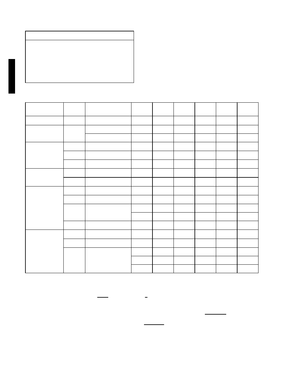
BLOCK DIAGRAM
ORDERING INFORMATION
PART NUMBER
PACKAGE
TEMPERATURE
GS9020-CFV
80 pin LQFP Tray
0∞C to 70∞C
GS9020-CTV
80 pin LQFP Tape
0∞C to 70∞C
DOUT[9:0]
FIFO_RESET
HVF
CLIP_TRS
HOSTIF
STANDARDS
INDICATOR
PCLK OUT
FRAMED
DATA [9:0]
SDOMODE
PCLKOUT
SDO
SDO
SDI
SDI
SCI
SCI
RESET
EDH
AND DATA
PROCESSING
CORE
ALIGNING
CONTROL
UNIT
10
10
7
TRS_ERR
SCRAMLER
DEDICATED
FLAG PORT
ANC_CHKSM
BUF
0
1
BUF
BUF
SERIAL TO
PARALLEL
CONVERTER
PARALLEL TO
SERIAL
CONVERTER
WITH SCRAMBLER
DESCRAMBLER
SYNC
DETECTOR
PRESCALER
5
4
GENLINX
TM
II
GS9020
Serial Digital Video Input Processor
521 - 66 - 05
2
G
S
902
0
ABSOLUTE MAXIMUM RATINGS
PARAMETER
VALUE
Supply Voltage
-0.3V to 6.0V
Input Voltage Range (any input)
-0.3 to V
DD
+0.3V
Operating Temperature Range
0∞C to 70∞C
Storage Temperature
-55∞C to 150∞C
Lead Temperature (soldering, 10 sec)
260∞C
DC ELECTRICAL CHARCTERISTICS
V
DD
= 5.0 V, T
A
= 0 - 70∞C unless otherwise shown.
PARAMETER
SYMBOL
CONDITIONS
MIN
TYP
MAX
UNITS
NOTES
TEST
LEVEL
Supply Voltage
V
DD
4.75
5.0
5.25
V
Supply Current
Unloaded
DD
270Mb/s
-
110
-
mA
540Mb/s
-
190
-
mA
High Speed Serial
Data and Clock
Inputs
V
CM
3.14
3.65
3.95
V
V
DIFFIN
450
800
1250
mV
R
PULLUP
-
75
-
1
Serial Data
Outputs
V
CM
-
2.7
-
V
V
DIFFOUT
-
800
-
mV
2
TTL Compatible
CMOS Inputs
V
ILMAX
-
-
0.8
V
V
IHMIN
2.0
-
-
V
IN
V
IN
= V
DD
or GND
-
-
150
µA
3
-
-
1
µA
4
C
IN
-
10
-
pF
TTL Compatible
CMOS Outputs
V
OLMAX
at
OUT
-
-
0.4
V
V
OHMIN
at
OUT
2.4
-
-
V
OUT
-
8
-
mA
5
-
4
-
mA
6
-
2
-
mA
7
NOTES
1. R
PULLUP
refers to the internal pullup resistor associated with the serial data and clock inputs (see Figure 4).
2. Assuming 100
differential termination resistor as shown in figure 7. Given V
DIFFOUT
= 800mV and a 100
termination, I
SDO
= 8mA.
3. The following inputs have internal pull-up resistors: SDOMODE. The following inputs have internal pull-down resistors:
ANC_CHKSM, FLYWDIS, FLAG_MAP, RESET, CRC_MODE, FIFOE/S AND HOSTIF_MODE.
4. All other inputs.
5. The following outputs have 8mA drivers (typical): PCLKOUT
6. The following outputs have 4mA drivers (typical): S[1:0], FL[4:0], ANC_DATA, DOUT[9:0], V, F[2:0], H, FIFO_RESET, TRS_ERR,
NO_EDH
7.The following outputs have 2mA drivers (typical): P[7:0], STD[3:0], INTERRUPT
521 - 66 - 05
3
G
S
9
020
AC ELECTRICAL CHARCTERISTICS
V
DD
= 5.0 V, T
A
= 0 - 70∞C unless otherwise shown.
PARAMETER
SYMBOL
CONDITIONS
MIN
TYP
MAX
UNITS
NOTES
TEST
LEVEL
Serial Input Clock
Frequency
SCI
-
-
540
MHz
Serial Data Input
Setup Time
t
SS
600
-
-
ps
1
Serial Data Input Hold
Time
t
SH
600
-
-
ps
1
Serial Data Output
Duty Cycle Distortion
-
5
-
%
Serial Output Jitter
540Mb/s at eye crossing
-
360
-
ps p-p
Serial Data Output
Rise Time
-
600
-
ps
Parallel Clock Output
Jitter
27MHz at 50% voltage
level
-
700
-
ps p-p
Input Timing
t
1
20
-
-
ns
2
t
2
-
-
9
ns
2
Output Delay Time
t
OD
with 25pF loading
T/2
-
T/2+7
ns
3
Output Hold Time
t
OH
with 25pF loading
T/2-3
-
-
ns
3
Output Setup Time
t
OS
with 25pF loading
T/2-7
-
-
ns
3
Flag Port Disable Time
t
FDIS
with 25pF loading
-
-
T/2+0.5
ns
Flag Port Enable Time
t
FEN
with 25pF loading
-
-
T/2+1
ns
I≤C Clock Frequency
SCL
-
-
400
kHz
Host Interface Setup
Time
t
HS
6
-
-
ns
4
Host Interface Hold
Time
t
HH
6
-
-
ns
4
Host Interface Output
Enable Time
t
HEN
with 25pF loading
-
-
21
ns
4
Host Interface Output
Disable Time
t
HDIS
with 25pF loading
-
-
10
ns
4
Reset Time Pulse
Width
t
RESET
100
-
-
ns
NOTES
1. The serial clock rising edge should occur at the centre of the data period for optimum performance. (See Figure 1)
2. Since the GS9020 does not have a parallel clock input, it is not possible to define timing details relative to it. Instead the GS9020 has
a parallel clock output and all timing information is relative to PCLKOUT. The flag port pins (FL[4:0], F_R/W, S[1:0]) are the only
inputs where the timing details are important. The timing requirements are shown in Figure 2.
3. These times are relative to the rising edge of PCLKOUT as shown in Figure 3. Note that the data transitions at the falling edge of
PCLKOUT. T is the parallel clock period in ns.
4. The Host Interface signals, P[7:0], R/W, A/D and CS are asynchronous to the parallel clock.
521 - 66 - 05
4
G
S
902
0
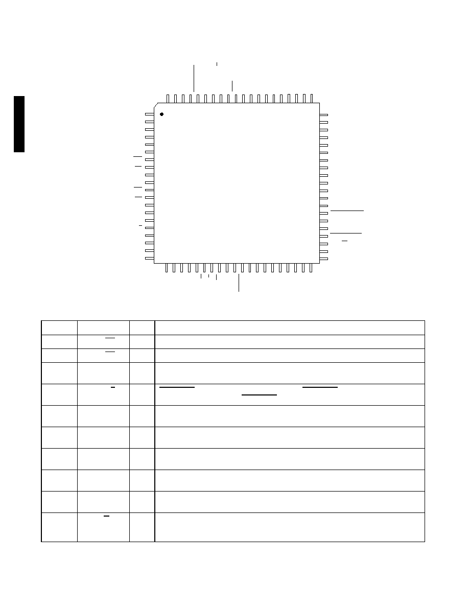
PIN CONNECTIONS
PIN DESCRIPTIONS
NUMBER
SYMBOL
TYPE
DESCRIPTION
6, 7
SDI, SDI
I
Differential serial data inputs.
10, 11
SCI, SCI
I
Differential serial clock inputs.
15
HOSTIF_MODE
I
Host interface mode select. When HIGH, the host interface is configured for I≤C mode. When
LOW, the host interface is configured for parallel port mode.
16
FIFOE/S
I
FIFO_RESET pulse control. When HIGH, the output FIFO_RESET pulse occurs on the EAV
word. When LOW, the output FIFO_RESET pulse occurs on the SAV word.
17
CRC_MODE
I
CRC_MODE enable. When HIGH, CRC_MODE is enabled. When LOW, CRC_MODE is
disabled.
18 - 20
P[7:5]
I/O
In parallel port mode, these are bits 7:5 of the host interface address/data bus. In I≤C mode,
these pins must be set LOW.
21
SCL/P4
I/O
In parallel port mode, this is bit 4 of the host interface address/data bus. In I≤C mode, this is the
serial clock input for the I≤C port.
22
SDA/P3
I/O
In parallel port mode, this is bit 3 of the host interface address/data bus. In I≤C mode, this is the
serial data pin for the I≤C port.
23 - 25
A[2:0]/P[2:0]
I/O
In parallel port mode, these are bits 2:0 of the host interface address/data bus. In I≤C mode,
these are input bits which define the I≤C slave address for the device..
26
R/W
I
Parallel port read/write control. When HIGH, the parallel port is configured as an output (read
mode). When LOW, the parallel port is configured as an input (write mode). In I≤C mode, this
pin must be set HIGH.
VDD
GND
GND
VDD
VDD
SDI
SDI
SDI
VDD
SDI
VDD
SCI
SCI
SCI
VDD
SCI
VDD
GND
HOSTIF_MODE
FIFOE/S
CRC_MODE
P7
P6
P5
DOUT9
DOUT8
DOUT7
DOUT6
DOUT5
DOUT4
DOUT3
DOUT2
DOUT1
VDD
GND
DOUT0
PCLKOUT
FIFO_RESET
NO_EDH
FLYWDIS
INTERRUPT
F_R/W
S0
S1
ANC_DATA
TRS_ERR
CLIP_TRS
ANC_CHKSM
BLANK_EN
SDOMODE
BYPASS_EDH
VBLANKS/L
SGND
SDO
SDO
SVDD
VDD
GND
FLAG_MAP
F2
F1
F0
H
V
SCL/P4
SDA/P3
A2/P2
A1/P1
A0/P0
R/W
A/D
CS
VDD
GND
RESET
STD3
STD2
STD1
STD0
FL4
FL3
FL2
FL1
FL0
1
2
3
4
5
6
7
8
9
10
11
12
13
14
15
16
17
18
19
20
80 79 78 77 76 75 74 73 72 71 70 69 68 67 66 65 64 63 62 61
21 22 23 24 25 26 27 28 29 30 31 32 33 34 35 36 37 38 39 40
60
59
58
57
56
55
54
53
52
51
50
49
48
47
46
45
44
43
42
41
GS9020
TOP VIEW

521 - 66 - 05
5
G
S
9
020
27
A/D
I
Parallel port address/data bus control. When HIGH, the parallel port is used for address input.
When LOW, the parallel port is used for data input or output. In I≤C mode, this pin must be set
LOW.
28
CS
I
Parallel port chip select. When CS is LOW and R/W is HIGH, the GS9020 drives the address/
data bus. When CS is LOW and R/W is LOW, the user should drive the address/data bus.
When CS is HIGH, the address/data bus is in a high impedance state (Hi - Z). In I≤C mode, this
pin must be set HIGH.
31
RESET
I
Reset. When LOW, the internal control circuitry is reset.
32 - 35
STD[3:0]
O
Video standards indication as described in section 1.4
36 - 40
FL[4:0]
I/O
EDH flag data port to allow access to the EDH flags.
41, 42
S[1:0]
I/O
Control bits which select whether FF, AP, or ANC EDH flags are active on the EDH flag data
port (FL[4:0]). In FLAG_MAP mode, the S[1:0] pins become outputs (see device description).
43
F_R/W
I
Flag port read/write control. When HIGH, FL[4:0] are configured as outputs allowing EDH flags
to be read from the device. When LOW, FL[4:0] are configured as inputs allowing EDH flags to
be overwritten in the outgoing EDH packet. In FLAG_MAP mode this pin must be set HIGH.
44
INTERRUPT
O
Interrupt output. This output goes low when EDH errors occur. This pin is an open drain output
and requires an external pullup resistor. If this output is not used, a pullup resistor is not
required.
45
FLYWDIS
I
Flywheel disable. When HIGH, the internal flywheel is disabled. When LOW, the internal
flywheel is enabled.
46
NO_EDH
O
No EDH present indication. When HIGH, indicates EDH packets are not present in the
incoming data stream.
47
FIFO_RESET
O
FIFO Reset output. Asserted LOW during the TRSID word for composite standards and the
EAV or SAV word for component standards.
48
PCLKOUT
O
Parallel clock output.
52-60,49
DOUT[9:0]
O
Parallel digital video data outputs.
61
V
O
Vertical sync indication.
62
H
O
Horizontal sync indication.
63 - 65
F[2:0]
O
Field indication. F2 is the MSB.
66
FLAG_MAP
I
FLAG_MAP mode enable. When HIGH, FLAG_MAP mode is enabled.
When LOW, FLAG_MAP mode is disabled.
70, 71
SDO/SDO
O
Differential serial data outputs.
73
VBLANKS/L
I
Vertical blanking interval control. For NTSC signals, when VBLANKS/L is set LOW the 19 line
blanking interval is selected and when set HIGH the 9 line blanking interval is selected. For
PAL D2 signals, when VBLANKS/L is set LOW the 17 line blanking interval is selected and
when set HIGH the 7 line blanking interval is selected. For PAL component signals VBLANKS/L
should be set LOW.
74
BYPASS_EDH
I
Bypass EDH control. When HIGH, the device allows the EDH packet to pass through
unaltered.
75
SDOMODE
I
Serial data output control. When LOW, the serial data output is re-serialized processed data.
When HIGH, the serial data output is the looped through serial input. After changing
SDOMODE, the GS9020 must be reset for proper operation.
76
BLANK_EN
I
Blanking enable. When LOW, incoming data words are set to appropriate blanking levels.
77
ANC_CHKSM
I
Ancillary checksum updating enable. When HIGH, ancillary checksum updating is enabled.
PIN DESCRIPTIONS
NUMBER
SYMBOL
TYPE
DESCRIPTION