GENNUM CORPORATION P.O. Box 489, Stn. A, Burlington, Ontario, Canada L7R 3Y3
Tel. +1 (905) 632-2996 Fax. +1 (905) 632-5946 E-mail: info@gennum.com
www.gennum.com
Revision Date: February 2000
Document No. 521 - 97 - 02
DATA SHEET
G
S
9
029
FEATURES
∑ SMPTE 259M compliant
∑ four isolated outputs (two complimentary pairs),
adjustable from 50mV-1000mV into 75
loads
∑ operational from 143Mb/s to 540Mb/s and beyond
∑ nominal 500ps rise/fall times
∑ precise ±7.5% output amplitudes
∑ 40% system power reduction over GS9007
∑ 75
on-chip input termination resistors
∑ input hysteresis
∑ operational down to 80mV input amplitude
∑ superior output isolation
∑ "Bus Through" expansion port for fan out
requirements
APPLICATIONS
4sc, 4:2:2 and 4:4:4:4 serial digital video co-axial
transmission interfaces from 143 to 540Mb/s; General
purpose cable driving applications (co-axial cable or UTP).
DESCRIPTION
The GS9029 is a second generation bipolar integrated
circuit designed to drive four 75
co-axial cables.
The GS9029 features two pairs of complementary outputs
whose amplitude is controlled within ±7.5%. The output
signal levels are also adjustable from 50mVp-p up to
1000mVp-p with little change in other performance
parameters. The amplitude of the output stage is varied by
adjusting the R
SET
resistor value. The patented current
mode outputs ensure superior output return loss and
minimal over shoot. The rise/fall time circuitry allows wide
range operation and provides symmetrical balanced
outputs to reject power supply noise. In addition high output
isolation ensures that the cable driver outputs are not
affected by the performance or status of other outputs.
Operational with input amplitudes as low as 80mV, the
GS9029 provides a robust serial interface.
The GS9029 is packaged in a 16 pin narrow SOIC and
operates from a single +5 or -5 volt supply. Typical system
power consumption is 320mW which is 40% less than the
GS9007.
BLOCK DIAGRAM
ORDERING INFORMATION
PART NUMBER
PACKAGE
TEMPERATURE
GS9029-CKD
16 pin SOIC Narrow
0∞C to 70∞C
GS9029-CTD
16 pin SOIC Tap
0∞C to 70∞C
SDI
75
75
BANDGAP REFERENCE & BIASING CIRCUIT
SDI
SDI/T
SDI/T
SDO0
SDO0
SDO1
SDO1
R
SET0
R
SET1
INPUT
DIFFERENTIAL
PAIR WITH
HYSTERESIS
OUTPUT STAGE &
RISE/FALL TIME
CONTROL CIRCUIT
GENLINX
TM
II
GS9029 Quad Output
Serial Digital Video Cable Driver
521 - 97 - 02
2
G
S
902
9
ABSOLUTE MAXIMUM RATINGS
PARAMETER
VALUE
Supply Voltage (V
S
=V
CC
-V
EE
)
5.5V
Input Voltage Range (any input)
-0.3V to (V
CC
+0.3)V
Maximum Die Temperature
125∞C
Operating Temperature Range
0∞C
T
A
70∞C
Storage Temperature Range
-65∞C
T
S
150∞C
Lead Temperature (soldering, 10 sec)
260∞C
DC ELECTRICAL CHARACTERISTICS
V
CC
= 5V, V
EE
= 0V, T
A
= 0∞C TO 70∞C unless otherwise specified. Specifications assume 800mV output amplitude into 75
terminated line.
PARAMETER
SYMBOL
CONDITIONS
MIN
TYP
MAX
UNITS
TEST
LEVEL
Supply Voltage
V
CC
Operating Range.
4.75
5.00
5.25
V
1
Power (system power)
P
S
Driving four 75
cables.
R
SET
= 54.9
.
-
320
350
mW
5
Supply Current
CC
Driving four 75
cables.
R
SET
= 54.9
.
-
64
70
mA
1
Common Mode Input
Voltage
V
CM_IN
2.4+(V
DIFF/2
)
-
V
CC
-(V
DIFF/2
)
V
6, 7
Differential Input
Voltage
V
DIFF
80
-
1000
mV
6, 7
Common Mode Output
Voltage Range
V
CM_OUT
-
V
CC
-V
OUT
-
V
5
Differential Output
Voltage
V
OUT
R
SET
= 54.9
740
800
860
mV
1
R
SET
= 43.2
925
1000
1075
mV
1
Input Hysteresis
-
25
-
mV
7
TEST LEVELS
1. Production test at room temperature and nominal supply voltage with guardbands for supply and temperature ranges.
2. Production test at room temperature and nominal supply voltage with guardbands for supply and temperature ranges using
correlated test.
3. Production test at room temperature and nominal supply voltage.
4. QA sample test.
5. Calculated result based on Level 1,2, or 3.
6. Not tested. Guaranteed by design simulations.
7. Not tested. Based on characterization of nominal parts.
8. Not tested. Based on existing design/characterization data of similar product.
521 - 97 - 02
3
G
S
9
029
AC ELECTRICAL CHARACTERISTICS
V
CC
= 5V, V
EE
= 0V, T
A
= 0∞C TO 70∞C unless otherwise specified. Specifications assume 800mV output amplitude into 75
terminated line.
PARAMETER
SYMBOL
CONDITIONS
MIN
TYP
MAX
UNITS
NOTES
TEST
LEVEL
Serial Data Bit Rate
143
-
540
Mb/s
1
Additive Jitter
270Mb/s
-
25
-
ps p-p
1, 2
7
540Mb/s
-
25
-
ps p-p
Output Rise/Fall Times
t
R
, t
F
20% - 80%
400
500
700
ps
1
Rise/Fall Times Mismatch
-
50
100
ps
5
Overshoot
-
5
-
% V
OUT
2
7
Duty Cycle Distortion
-
50
100
ps
1
Output Return Loss
5MHz - 540MHz
-
17
-
dB
2
7
NOTES
1. 6
additive jitter measuring Pseudo random bit sequence (2
23
-1).
2. Measured with Gennum Evaluation Board (EB9029V1).
TEST LEVELS
1. Production test at room temperature and nominal supply voltage with guardbands for supply and temperature
ranges.
2. Production test at room temperature and nominal supply voltage with guardbands for supply and temperature
ranges using correlated test.
3. Production test at room temperature and nominal supply voltage.
4. QA sample test.
5. Calculated result based on Level 1,2, or 3.
6. Not tested. Guaranteed by design simulations.
7. Not tested. Based on characterization of nominal parts.
8. Not tested. Based on existing design/characterization data of similar product.
521 - 97 - 02
4
G
S
902
9
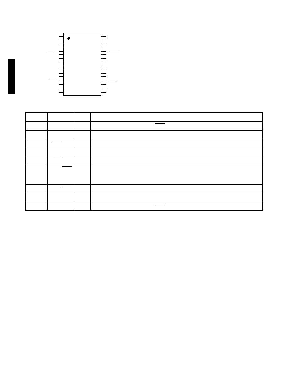
PIN CONNECTIONS
R
SET1
V
CC
SDO1
SDO1
NC
NC
SDI
SDI
R
SET0
V
EE
SDO0
SDO0
NC
NC
SDI/T
SDI/T
GS9029
TOP VIEW
1
2
3
4
5
6
7
8
16
15
14
13
12
11
10
9
PIN DESCRIPTIONS
NUMBER
SYMBOL
TYPE
DESCRIPTION
1
R
SET1
I
Amplitude setting resistor for SDO1, SDO1.
2
V
CC
Most positive supply voltage.
3, 4
SDO1,SDO1
O
Second differential serial output (inverse and true).
5,6,11,12
NC
No connect.
7, 8
SDI,SDI
I
Serial data inputs (inverse and true).
9, 10
SDI/T, SDI/T
I
Dual mode pin:
a) "Bus Through" pins for serial data inputs when additional GS9029s are used on the same bus.
b) Termination pins when using a single GS9029, or when the device is the last on an input bus.
13, 14
SDO0,SDO0
O
First differential serial output (true and inverse).
15
V
EE
Most negative supply voltage.
16
R
SET0
I
Amplitude setting resistor for SDO0, SDO0.
521 - 97 - 02
5
G
S
9
029
TYPICAL PERFORMANCE CURVES (V
S
= 5V, T
A
= 25∞C unless otherwise shown. Devices guard band tested to 70∞C only.)
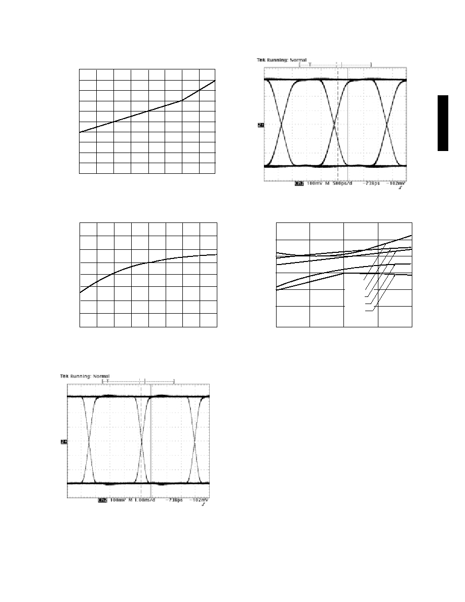
Fig. 1 Rise/Fall vs. Temperature
Fig. 2 Serial Data Output Level vs. Temperature
Fig. 3 270Mb/s Eye Diagram
Fig. 4 540Mb/s Eye Diagram
Fig. 5 Peak to Peak Additive Jitter vs. Temperature
530
525
520
515
510
505
500
495
490
485
480
TIME (ps)
0
10
20
30
40
50
60
70
80
TEMPERATURE (∞C)
1.62
1.61
1.60
1.59
1.58
OUTPUT LEVEL (V)
0
10
20
30
40
50
60
70
80
TEMPERATURE (∞C)
40
35
30
25
20
15
10
JITTER p-p (ps)
0
20
40
60
80
TEMPERATURE (∞C)
360Mb/s
177Mb/s
143Mb/s
540Mb/s
270Mb/s