
www.gennum.com
GS9064A HD-LINXÆ II
Adaptive Cable Equalizer
GS9064A Data Sheet
37325 - 0
December 2005
1 of 16
Features
∑
SMPTE 259M compliant
∑
Automatic cable equalization
∑
Supports DVB-ASI at 270Mb/s
∑
Pb-free and RoHS compliant
∑
Manual bypass (useful for low data rates with slow
rise/fall times)
∑
Performance optimized for 270Mb/s
∑
Typical maximum equalized length of Belden
1694A cable: 350m at 270Mb/s
∑
50
differential output (with internal 50 pull-ups)
∑
Manual output mute or programmable mute based
on max cable length adjust
∑
Cable length indicator for SMPTE 259M inputs
∑
Single 3.3V power supply operation
∑
Operating temperature range: 0∞C to +70∞C
Applications
∑
SMPTE 259M Coaxial Cable Serial Digital
Interfaces.
Description
The GS9064A is a second-generation high-speed
BiCMOS integrated circuit designed to equalize and
restore signals received over 75
co-axial cable.
The GS9064A is designed to support SMPTE 259M,
and is optimized for performance at 270Mb/s.
The GS9064A features DC restoration to compensate
for the DC content of SMPTE pathological test patterns.
The device also incorporates a Cable Length Indicator
(CLI) that provides an indication of the amount of cable
being equalized.
A voltage programmable mute threshold (MCLADJ) is
included to allow muting of the GS9064A output when
an approximate selected cable length is reached for
SMPTE 259M signals. This feature allows the GS9064A
to distinguish between low amplitude SD-SDI signals
and noise at the input of the device.
The bidirectional CD/MUTE pin indicates the presence
of a valid signal at the input of the GS9064A in addition
to functioning as a mute control input. The outputs of the
GS9064A will be forced to a mute state when an invalid
input reference signal is applied to the input of the
device or the application layer sets the CD/MUTE pin
HIGH. If the application layer forces CD/MUTE LOW,
the serial digital output of the device will always be
active.
Power consumption is typically 265mW using a 3.3V
power supply.
The GS9064A is Pb-free, and the encapsulation
compound does not contain halogenated flame
retardant (RoHS Compliant).

GS9064A Data Sheet
37325 - 0
December 2005
2 of 16
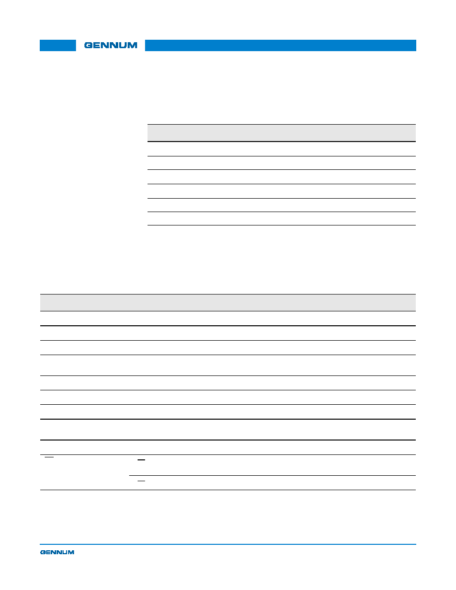
GS9064A Functional Block Diagram
Contents
Features ........................................................................................................................1
Applications...................................................................................................................1
Description ....................................................................................................................1
1. Pin Out ......................................................................................................................3
1.1 GS9064A Pin Assignment ..............................................................................3
1.2 GS9064A Pin Descriptions .............................................................................4
2. Electrical Characteristics...........................................................................................5
2.1 Absolute Maximum Ratings ............................................................................5
2.2 DC Electrical Characteristics ..........................................................................5
2.3 AC Electrical Characteristics ...........................................................................6
2.4 Solder Reflow Profiles .....................................................................................7
3. Input / Output Circuits ...............................................................................................9
4. Detailed Description ................................................................................................11
4.1 Serial Digital Inputs .......................................................................................11
4.2 Cable Equalization ........................................................................................11
4.3 Programmable Mute Output and Cable Length Indicator .............................12
4.4 Mute and Carrier Detect ................................................................................13
5. Application Information............................................................................................14
5.1 Typical Application Circuit .............................................................................14
6. Package & Ordering Information.............................................................................15
6.1 Package Dimensions ....................................................................................15
6.2 Packaging Data .............................................................................................15
6.3 Ordering Information .....................................................................................15
7. Revision History ......................................................................................................16
CABLE LENGTH INDICATOR/ADJUSTOR
CARRIER DETECT
MUTE
EQUALIZER
DC RESTORE
OUTPUT
AGC
CLI
CD/MUTE
SDO
BYPASS
SDO
SDI
SDI
MCLADJ

GS9064A Data Sheet
37325 - 0
December 2005
3 of 16
1. Pin Out
1.1 GS9064A Pin Assignment
Figure 1-1: 16-Pin SOIC
CLI
V
CC
V
EE
SDI
SDI
V
EE
AGC+
AGC-
CD/MUTE
V
CC
V
EE
SDO
SDO
V
EE
MCLADJ
BYPASS
GS9064A
1
2
3
4
5
6
7
8
16
15
14
13
12
11
10
9
(top view)

GS9064A Data Sheet
37325 - 0
December 2005
4 of 16
1.2 GS9064A Pin Descriptions
Table 1-1: GS9064A Pin Descriptions
Pin Number
Name
Timing
Type
Description
1
CLI
Analog
Output
Cable Length Indicator.
An analog voltage will be output proportional to the cable length
connected to the serial digital input.
2, 15
V
CC
Analog
Power
Most positive power supply connection.
Connect to +3.3V DC.
3, 6, 11, 14
V
EE
Analog
Power
Most negative power supply connection.
Connect to GND.
4, 5
SDI, SDI
Analog
Input
Serial digital differential input.
7, 8
AGC+,
AGC-
Analog
≠
External AGC capacitor.
Connect pin 7 and pin 8 together through a 1uF capacitor.
9
BYPASS
Not
Synchronous
Input
Forces the Equalizing and DC RESTORE stages into bypass mode
when HIGH. No equalization occurs in this mode.
10
MCLADJ
Analog
Input
Maximum cable length adjust.
Adjusts the approximate maximum amount of cable to be equalized
(from 0m to the maximum cable length). The output is muted (latched to
the last state) when the maximum cable length is achieved.
12, 13
SDO, SDO
Analog
Output
Equalized serial digital differential output.
16
CD/MUTE
Not
Synchronous
Bidirectional
STATUS SIGNAL OUTPUT / CONTROL SIGNAL INPUT
levels are LVCMOS/LVTTL compatible.
OUTPUT (CD):
Indicates the presence of a valid input signal. When the CD pin is LOW,
a valid input signal has been detected. When this pin is HIGH, the input
signal is invalid. If CD is set HIGH, the serial digital output of the device
will be forced to a steady state (latched to the last state).
NOTE: This pin will indicate loss of carrier for data rates > 19Mb/s.
INPUT (MUTE):
When the MUTE pin is set HIGH by the application interface, the serial
digital output of the device will be forced to a steady state (latched to the
last state). When the MUTE pin is set LOW, the serial digital output of
the device will be active.
NOTE: The CD/MUTE pin is not functional when BYPASS is set HIGH.
GS9064A Data Sheet
37325 - 0
December 2005
5 of 16
2. Electrical Characteristics
2.1 Absolute Maximum Ratings
2.2 DC Electrical Characteristics
Parameter
Value
Supply Voltage
-0.5V to +3.6 V
DC
Input ESD Voltage
2kV
Storage Temperature Range
-50∞C < T
s
< 125∞C
Input Voltage Range (any input)
-0.3 to (V
CC
+0.3)V
Operating Temperature Range
0∞C to 70∞C
Reflow Temperature
260∞C
Table 2-1: DC Electrical Characteristics
V
DD
= 3.3V, T
A
= 0∞C to 70∞C, unless otherwise shown
Parameter
Symbol
Conditions
Min
Typ
Max
Units
Notes
Supply Voltage
V
CC
≠
3.135
3.3
3.465
V
±5%
Power Consumption
P
D
T
A
= 25∞C
≠
265
≠
mW
≠
Supply Current
I
s
T
A
= 25∞C
≠
80
≠
mA
≠
Output Common Mode
Voltage
V
CMOUT
T
A
= 25∞C
≠
V
CC
-
V
SDO
/2
≠
V
≠
Input Common Mode Voltage
V
CMIN
T
A
= 25∞C
≠
1.75
≠
V
≠
CLI DC Voltage (0m)
≠
T
A
= 25∞C
≠
2.5
≠
V
≠
CLI DC Voltage (no signal)
≠
T
A
= 25∞C
≠
1.9
≠
V
≠
MCLADJ DC Voltage (to mute
signal)
≠
0m, T
A
= 25∞C
≠
1.3
≠
V
≠
MCLADJ Range
≠
T
A
= 25∞C
≠
0.4
≠
V
≠
CD/MUTE Output Voltage
V
CD/MUTE(OH)
Carrier not
present
2.4
≠
≠
V
≠
V
CD/MUTE(OL)
Carrier present
≠
≠
0.4
V
≠