-V
S
+V
S
COMP
C
OS1
C
OS2
S1
V
REF
S2
V
C
GND
OUT
B
OS2
-IN B
+IN B
B
OS1
A
OS2
-IN A
+IN A
A
OS1
R
EXT
20
11
10
PIN 1
TOP VIEW
Document No. 520 - 25 - 4
DATA SHEET
GT4122 Video Multiplier
GENNUM CORPORATION P.O. Box 489, Stn A, Burlington, Ontario, Canada L7R 3Y3 tel. (905) 632-2996 fax: (905) 632-5946
Japan Branch: A-302, Miyamae Village, 2-10-42 Miyamae, Suginami-ku, Tokyo 168, Japan tel. (03) 3334-7700 fax: (03) 3247-8839
DESCRIPTION
The GT4122 multiplier is a monolithic dual-channel,
broadcast quality video mixer.
Featuring two wideband video inputs and a single control
input, the GT4122 achieves high quality video mixing of
the two video input signals to a single output by implementing
the function:
V
OUT
= V
A
∑ V
C
+ V
B
(1 - V
C
)
where V
C
is the control input voltage, which may be
varied continuously over the control range and V
A
and V
B
are the video input signals.
The GT4122 operates with power supply voltages of
±
10
volts and typically draws 24 mA of current. The GT4122
is available in a 20 pin DIP and 20 pin SOIC packaging.
An Application Note entitled `Using the GT4122 and
GT4124 Video Mixer ICs' (Gennum Document 520-44) is
available from Gennum Corporation.
FEATURES
∑ broadcast quality video multiplier
∑ 30 MHz at -1.0 dB video and control channel bandwidth
∑ one external frequency compensation adjustment
∑ ultra low differential gain and differential phase,
(typically 0.01 % and 0.01 deg.)
∑ external DC offset and span trims
∑ 20 pin PDIP and SOIC packaging
APPLICATIONS
∑ Production switcher video mixers
∑ Linear Keyers
Part No.
Package Type
Temperature
GT4122 - CDF
20 PDIP
0
∞
to 70
∞
C
GT4122 - CKF
20 SOIC
0
∞
to 70
∞
C
ORDERING INFORMATION
PIN CONNECTIONS
TOP VIEW
20 PIN DIP / SOIC
R
EXT
C
OS1
V
REF
C
OS2
V
C
+
-
-
V
S
GND
A
OS2
+
IN A
-
IN A
B
OS2
-
IN B
V
CA
=0.5 + V
K
+
IN B
+
V
S
B
OS1
A
OS1
BIAS
AMP 3
S1
S 2
COMP
OUT
V
NOM
AMP 1
AMP 2
+
-
+
-
XA
V
CB
=0.5 - V
K
XB
+
+
AMP 4
-
+
A
K
0.5V
2
3
+
-
+
-
+
+
V
K
-
V
K
+
+
1
V
NOM
Device Function: V
OUT
= V
INA
∑ [V
NOM
+ A
K
(V
C
- V
REF
)] + V
INB
∑ [V
NOM
- A
K
(V
C
- V
REF
)]
FUNCTIONAL BLOCK DIAGRAM
1
-V
S
negative supply voltage
2
+V
S
positive supply voltage
3
COMP output freq'y comp'n R-C
4
C
OS1
control input offset adjust
5
C
OS2
control input offset adjust
6
S1
span adjust
7
V
REF
0.5volt reference input
8
S2
span adjust
9
V
C
control signal input
10
GND ground
11
R
EXT
current setting resistor
12
A
OS1
A black level adjust (OFFSET)
13
+IN A A video + input signal
14
-IN A A video - signal input
15
A
OS2
A black level adjust (OFFSET)
16
B
OS1
B black level adjust (OFFSET)
17
+IN B B video + signal input
18
-IN B B video - signal input
19
B
OS2
B black level adjust (OFFSET)
20
OUT
multiplier output
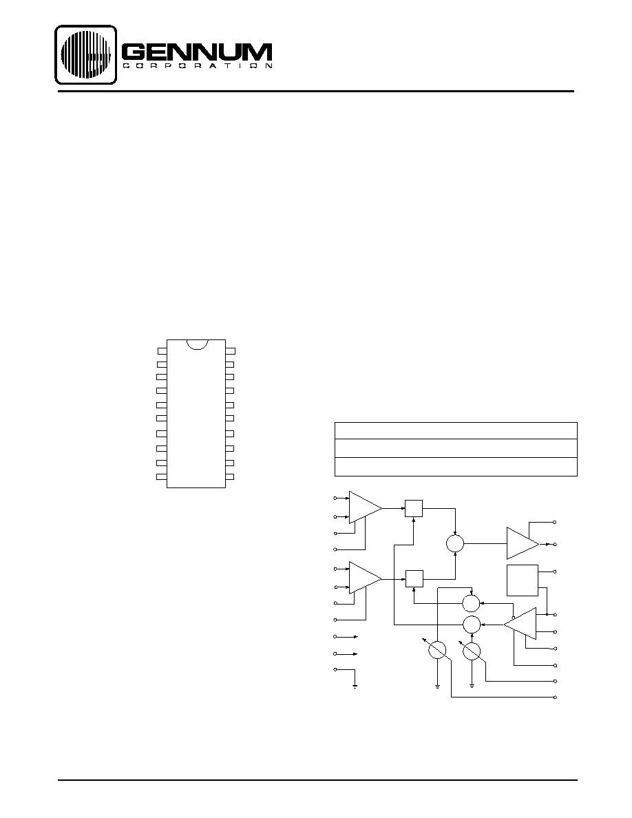
PIN DESIGNATION
Revision Date: January 1994.

520 - 25 - 4
2
PARAMETER
VALUE
Supply Voltage (V
S
)
±
13.5 V
Operating Temperature Range
0
∞
C
T
A
70
∞
C
Storage Temperature Range
-65
∞
C
T
S
150
∞
C
Lead Temperature (Soldering, 10 Sec)
260
∞
C
Video Input Voltage (V
A
,V
B
) to ground
±
5 V
Control Input Voltage (V
C
) to ground
±
5 V
Video Input Differential Voltage (V
A
- V
B
)
±
5 V
Control Input Differential Voltage (V
C
-V
REF
)
±
5 V
ABSOLUTE MAXIMUM RATINGS
ELECTRICAL CHARACTERISTICS
PARAMETER
SYMBOL
CONDITIONS
MIN
TYP
MAX
UNITS
Supply Voltage
±
V
S
Operating Range
±
9
±
10
±
12
volts
+ Supply Current
I
+
R
EXT
= 1 k
-
24
28
mA
- Supply Current
I
-
R
EXT
= 1 k
-
18
20
mA
Bandwidth
BW at
±
0.1 dB V
SIG
=150 mVp-p
25
30
-
MHz
Frequency Response
DC - 10 MHz
-
±
0.05
-
dB
Differential Gain
g
V
IN
= 40 IRE at 3.58 MHz
-
0.01
0.03
%
Differential Phase
p
V
IN
= 40 IRE at 3.58 MHz
-
0.01
0.03
degrees
Signal to Noise
S/N
V
SIG
= 1 volt, BW = 5 MHz
64
70
-
dB
Gain - open loop
A
OL
100 kHz (þ = 0%)
54
60
66
dB
Gain - closed loop
A
CL
100 kHz (þ = 100%)
-0.01
-0.005
-
dB
Delay
td
SIG
-
-
10
ns
Off Isolation & Crosstalk
V
A or B
/V
O
SIG
= 5 MHz (see note 1)
80
85
-
dB
V
C
/V
A or B
SIG
= 5 MHz (see note 2)
90
95
-
dB
Bandwidth
BW
at
±
0.1 dB V
SIG
=150 mVp-p
25
30
-
MHz
Delay
t
d CONT
-
-
10
ns
Linearity
-
1
-
%
Control Breakthrough
V
CONT
= 0-1 V = 1-10 MHz
-
-55
-50
dB
Crossfade Balance
V
CONT
= 0-1 V = 3.58 MHz
-
3
5
mVpp
Control Range
V
CONT
0
-
+5
V
NOTE:
1 V
A or B
=1 Vp-p output taken from OUTPUT
2 V
CONT
=1 Vp-p output taken from V
A
or
V
B
(+V
S
= -V
S
=10V, 0
∞
C
T
A
70
∞
C unless otherwise shown)
SIGNAL
CHANNEL
POWER
SUPPLIES
CONTROL
CHANNEL

520 - 25 - 4
3
Referring to the block diagram, the input signals are applied
to conventional differential amplifiers (AMP1 and AMP2).
Each amplifier has provisions for individually adjusting the
DC offset (OFFSET).
Following each input amplifier, the signals are applied to
linear multiplier circuits (XA and XB) whose outputs are the
product of the incoming signals and controlling voltages (V
CA
)
or (V
CB
). The controlling voltage V
CA
is the sum of a nominal
0.5V source (V
NOM
) and a variable source V
K
while V
CB
is made
up of the sum of the nominal voltage V
NOM
and -V
K
.
V
K
and -V
K
are themselves proportional to the difference
between an externally applied reference voltage (V
REF
) and
an externally applied CONTROL voltage (V
C
). The voltages V
K
and -V
K
are produced by a differential amplifier (AMP3) whose
gain is A
K
. This gain can be altered by two external resistors,
R
EXT
and R
SPAN
according to the following formula:
Note that R
EXT
is connected between the R
EXT
pin and ground
and R
SPAN
is connected between the pins S1 and S2.
Each of the voltages (+V
K
and -V
K
) is applied to summing
circuits (
2 and
3) whose second inputs are DC voltage
sources that can also be slightly varied. The nominal value of
these voltage sources is 0.5 volts.
When they are exactly 0.5V and when V
C
= V
REF
, the gain of
each signal channel of the mixer is 0.5 (50%).
By connecting the ends of an external potentiometer
(CONTROL OFFSET) between the offset pins COS1 and
COS2, the voltage sources can be altered differentially. If a
second potentiometer (50% GAIN) is connected between the
wiper of the CONTROL OFFSET potentiometer and the supply
voltage, the voltage sources can be varied in a common
mode fashion. In this way not only can the control range of
the mixer be varied but also the point at which 50% of each
input signal appears at the output.
The outputs from the multiplier circuits (XA and XB) are then
applied to a summing circuit (
1) whose output feeds a
wideband amplifier (AMP4) and presents the mixed signals to
the outside world.
Although there are two separate differential inputs, the usual
operational amplifier gain-setting methods can be applied to
determine the closed loop gain of the mixer. Usually the
mixer will be configured for unity gain by connecting both
inverting inputs (-IN A , -IN B) to the common output (OUT). In
this case, the general transfer function is:
V
O
= V
A
∑[V
NOM
+ A
K
∑(V
C
- V
REF
)] + V
B
∑[V
NOM
- A
K
∑(V
C
-
V
REF
)]
(Unity gain configuration)
Where V
A
and V
B
are the input analog signals applied to +IN A
and +IN B respectively, and V
C
is the CONTROL voltage.
Note that V
NOM
ranges between 0.45V < V
NOM
< 0.55.
DETAILED DESCRIPTION
0.85 ∑ R
EXT
A
K
---------- [1k
< R
EXT
< 3k
]
R
SPAN
R
EXT
C
OS1
V
REF
C
OS2
V
C
+
-
-
V
S
GND
A
OS2
+
IN A
-
IN A
B
OS2
-
IN B
V
CA
=0.5 + V
K
+
IN B
+
V
S
B
OS1
A
OS1
BIAS
AMP 3
S1
S 2
COMP
OUT
V
NOM
AMP 1
AMP 2
+
-
+
-
XA
V
CB
=0.5 - V
K
XB
+
+
AMP 4
-
+
A
K
0.5V
2
3
+
-
+
-
+
+
V
K
-
V
K
+
+
1
V
NOM
Device Function: V
OUT
= V
INA
∑ [V
NOM
+ A
K
(V
C
- V
REF
)] + V
INB
∑ [V
NOM
- A
K
(V
C
- V
REF
)]
The GT4122 is a broadcast quality monolithic inte-
grated circuit specifically designed to linearly mix two
video signals under the control of a third signal.
FUNCTIONAL BLOCK DIAGRAM

520 - 25 - 4
4
For normal video mixer operation, the control range (SPAN) is
usually 0 to 1V and will occur when A
K
=1, V
REF
= 0.5V and
V
NOM
=0.5 volts. A change in V
C
from 0 to 1V will then produce
an effect such that the output signal contains 100% of Channel
B when V
C
is 0V and 100% of Channel A when V
C
is 1 volt. For
the above conditions, the general unity gain transfer function
reduces to:
V
O
= V
A
∑V
C
+ V
B
∑(1-V
C
)
Since the operation of the mixer is limited to two quadrants, no
signal inversions occur if the control voltage exceeds the
range zero to one volt in either direction. The topology is
designed so that once the control voltage reaches either end
of its range, the channel which is ON remains fully ON and the
OFF channel remains fully OFF.
0.1
or LINK
GT4122
CONTROL
OFFSET
RV2
100
C3
0.1
COUT
-5V
C6 0.1
ROUT
10k or
OPEN
+5V
B VIDEO INPUT
CONTROL INPUT
Z1
6.2V
R3
1k
RV1
200
R2
1k
C2 0.1
R1
560
(0.5V)
R4
5.6k
50%
GAIN
B BLACK
LEVEL
ADJUST
A BLACK
LEVEL
ADJUST
75
if required
RV4
500
RV5
500
1
2
4
3
17
18
19
20
+10V
-10V
-V
S
GND
COMP
C
OS1
OUT
B
OS2
6
5
7
15
16
14
+IN B
S1
-IN B
A
OS2
-IN A
9
8
10
12
13
S2
V
REF
+IN A
A
OS1
11
C5
47
-10V
C5
47
C1 0.1
5 - 25pF
CCOMP
RV6
1k
VREF
ADJUST
RV3
SPAN
ADJUST
C5
0.1
+V
S
C
OS2
V
C
R
EXT
B
OS1
C7 0.1
A VIDEO INPUT
75
if required
75
if required
IC2
CLC110
1
4
5
8
+
+
VIDEO OUT
1K
NOTE: C5 is used when the CONTROL VOLTAGE (V
C
) is derived from a power supply.
All resistors in ohms, all capacitors in
µ
F unless otherwise stated.
Fig. 1 Test Circuit

520 - 25 - 4
5
Gennum Corporation assumes no responsibility for the use of any circuits described herein and makes no representations that they are free from patent infringement.
© Copyright April 1991 Gennum Corporation. All rights reserved. Printed in Canada.
DOCUMENT
IDENTIFICATION
PRODUCT PROPOSAL
This data has been compiled for market investigation purposes
only, and does not constitute an offer for sale.
ADVANCE INFORMATION NOTE
This product is in development phase and specifications are
subject to change without notice. Gennum reserves the right to
remove the product at any time. Listing the product does not
constitute an offer for sale.
PRELIMINARY DATA SHEET
The product is in a preproduction phase and specifications are
subject to change without notice.
DATA SHEET
The product is in production. Gennum reserves the right to make
changes at any time to improve reliability, function or design, in
order to provide the best product possible.
CAUTION
ELECTROSTATIC
SENSITIVE DEVICES
DO NOT OPEN PACKAGES OR HANDLE
EXCEPT AT A STATIC-FREE WORKSTATION
GAIN (dB)
FREQUENCY (MHz)
-20
-30
-40
-50
-60
-70
-80
-90
-100
1
100
1
10
100
V
IN
= 1 Vp-p
CH-A
CH-B
GAIN (dB)
1
60
0.5
0.4
0.3
0.2
0.1
0.0
-0.1
-0.2
-0.3
-0.4
-0.5
1
10
60
FREQUENCY (MHz)
CH-B
V
IN
= 150 mVp-p
R
COMP
= 560
C
COMP
= 18 pF
CH-A
Fig. 3 Crosstalk vs Frequency
Fig. 2 Frequency Response
dg
(%) /
dp
(deg)
FREQUENCY (MHz)
0.03
0.02
0.01
0.00
-0.01
-0.02
-0.03
1
3
5
10
dg
dp
Fig. 4 Differential Gain & Phase vs Frequency
GAIN (dB)
1
10
-20
-30
-40
-50
-60
-70
-80
-90
-100
1
3
5
10
V
C
= 1Vp-p+0.5 VDC
REF = 1Vp-p (0dB)
FREQUENCY (MHz)
Fig. 5 Crossfade Balance vs Frequency
TYPICAL PERFORMANCE CURVES FOR GT4122
(Unless otherwise shown, V
S
=
±
10 V, R
L
= 10 k
)