 | –≠–ª–µ–∫—Ç—Ä–æ–Ω–Ω—ã–π –∫–æ–º–ø–æ–Ω–µ–Ω—Ç: GX434CDB | –°–∫–∞—á–∞—Ç—å:  PDF PDF  ZIP ZIP |

GENNUM CORPORATION P.O. Box 489, Stn A, Burlington, Ontario, Canada L7R 3Y3 tel. (905) 632-2996 fax: (905) 632-5946
Japan Branch: A-302 M i yamae Vi l l age, 2≠10≠42 M i yamae, Suginami≠ku, Tokyo 168, Japan tel. (03) 3334-7700 fax (03) 3247-8839
X = DON'T CARE
CS A1 A0 OUTPUT
0 0 0 IN 0
0 0 1 IN 1
0 1 0 IN 2
0 1 1 IN 3
1 X X HI - Z
TRUTH TABLE
X
X
X
X
CHIP
SELECT
2 TO 4 DECODER
LOGIC
FUNCTIONAL BLOCK DIAGRAM
OUTPUT
CS
IN 0
IN 1
IN 2
IN 3
A 0
A 1
AVAILABLE PACKAGING
14 pin DIP and 16 pin SOIC (wide)
DATA SHEET
CIRCUIT DESCRIPTION
The GX434 is a high performance low cost monolithic 4x1
video multiplexer incorporating four bipolar switches with a
common output, a 2 to 4 address decoder and fast chip select
circuitry. The chip select input allows for multi-chip paralleled
operation in routing matrix applications. The chip is selected
by applying a logic 0 on the chip select input.
Unlike devices using MOS bilateral switching elements, these
bipolar circuits represent fully buffered, unilateral transmission
paths when selected. This results in extremely high output to
input isolation. They also feature fast make-before-break
switching action. These features eliminate such problems as
switching 'glitches' and output-to-input signal feedthrough.
The GX434 operates from
±
7 to
±
13.2 volt DC supplies. They
are specifically designed for video signal switching which
requires extremely low differential phase and gain. Logic
inputs are TTL and 5 volt CMOS compatible providing address
and chip select functions. When the chip is not selected, the
output goes to a high impedance state.
GX434 Monolithic 4x1
Video Multiplexer
Document No. 510 - 34 - 2
FEATURES
∑
low differential gain: 0.03% typ. at 4.43 MHz
∑
low differential phase: 0.012 deg. typ. at 4.43 MHz
∑
low insertion loss: 0.05 dB max at 100 kHz
∑
low disabled power consumption: 5.2 mW typ.
∑
high off isolation: 110 dB at 10 MHz
∑
all hostile crosstalk @ 5 MHz, 97 dB typ.
∑
bandwidth (-3dB) with 30 pF load, 100 MHz typ.
∑
fast make-before-break switching: 200 ns typ.
∑
TTL and 5 volt CMOS compatible logic inputs
∑
low cost 14 pin DIP and16 pin SOIC packages
∑
optimised performance for NTSC, PAL and SECAM
applications
APPLICATIONS
Glitch free analog switching for...
∑ High quality video routing
∑ A/D input multiplexing
∑ Sample and hold circuits
∑ TV/ CATV/ monitor switching
IN 0
GND
IN 1
GND
GND
IN 2
IN 3
NC
NC
+8V
-8V
NC
O/P
CS
A1
AO
TOP VIEW
PIN 1
8
16
9
PIN CONNECTION
16 PIN SOIC
IN 0
PIN CONNECTION
14 PIN DIP
GND
IN 1
GND
IN 3
GND
IN 2
AO
+8V
A1
CS
O/P
NC
-8V
PIN 1
7
8
14
TOP VIEW
R
EXT
R
EXT
GX434
(wide)
PIN CONNECTIONS

510 -34 -2
2
PARAMETER
SYMBOL
CONDITIONS MIN TYP MAX UNITS
Supply Voltage
±
V
S
7
8
13.2
V
DC
I
+
Chip selected (CS=0)
-
10.5
11.5
mA
SUPPLY
Chip not selected (CS=1)
-
0.4
0.58
mA
Supply current
I
-
Chip selected (CS=0)
-
10.2
11.2
mA
Chip not selected (CS=1)
-
0.25
0.38
mA
Analog Output
V
OUT
Extremes before clipping
-
+2
-
occurs.
-
-1.2
V
Analog Input Bias
I
BIAS
-
22
-
µ
A
Current
STATIC
Output Offset Voltage
V
OS
T
A
= 25
∞
C, 75
resistor
on each input to gnd
0
7
14
mV
Output Offset Voltage
V
OS
/
T
-
+50
+200
µ
V/
∞
C
Drift
R
EXT
= 33.2 k
, 1%
ORDERING INFORMATION
Part Number
Package Type Temperature Range
GX434 ≠ ≠ CDB
14 Pin DIP
0
∞
to 70
∞
C
GX434 ≠ ≠ CKC
16 Pin SOIC
0
∞
to 70
∞
C
GX434 ≠ ≠ CTC
Tape 16 Pin SOIC
0
∞
to 70
∞
C
ABSOLUTE MAXIMUM RATINGS
Parameter
Value & Units
Supply Voltage
±
13.5V
Operating Temperature Range
0
∞
C
T
A
70
∞
C
Storage Temperature Range
-65
∞
C
T
S
150
∞
C
Lead Temperature (Soldering, 10 Sec)
260
∞
C
Analog Input Voltage
-4V
V
IN
+2.4V
Analog Input Current
50
µ
A AVG, 10 mA peak
Logic Input Voltage
-4V
V
L
+5.5V
Fig.1 Crosspoint Equivalent Circuit
Fig. 2 Disabled Crosspoint Equivalent Circuit
CS
# 2
# 3
# 4
ELECTRICAL CHARACTERISTICS
(V
S
=
±
8V DC, 0
∞
C < T
A
< 70
∞
C, C
L
= 30 pF, R
L
= 10k
unless otherwise shown.)
CAUTION
ELECTROSTATIC SENSITIVE DEVICES
DO NOT OPEN PACKAGES OR HANDLE
DEVICES EXCEPT AT A
STATIC-FREE WORKSTATION
0.65V
2pF
600
1.3 V
+
1.2k
1.5pF
V
IN
V
OUT
12pF
Common
C
OUT
OUT
+Vcc
-V
CS
IN
CS
+
16pF
0.7pF
0.7pF
0.7pF
0.7pF
3mA
GX434

510 -34 -2
3
R
EXT
= 33.2k
, 1%
GX434
PARAMETER
SYMBOL
CONDITIONS
MIN
TYP
MAX
UNITS
Crosspoint Selection
t
ADR-ON
Control input to appearance
130
200
270
ns
Turn-On Time
of signal at the output.
Crosspoint Selection
t
ADR-OFF
Control input to disappear-
390
600
800
ns
Turn-Off Time
ance of signal at output.
Chip Selection
t
CS-ON
Control input to appearance
200
300
400
ns
Turn-On Time
of signal at output.
Chip Selection
t
CS-OFF
Control input to disappear-
460
700
940
ns
Turn-Off Time
ance of signal at output.
LOGIC
Logic Input
V
IH
1
2.0
-
-
V
Thresholds
V
IL
0
-
-
1.1
V
Address Input
I
BIAS(ADR)
Chip selected A0,A1 = 1
-
-
5.0
µ
A
Bias Current
Chip selected A0,A1 = 0
-
-
0.1
nA
Chip Select Bias
I
BIAS(CS)
CS = 1
-
-
1.0
nA
Current
CS = 0
-
-
30
µ
A
Insertion Loss
I.L.
1V p-p sine or sq. wave at
0.025
0.03
0.04
dB
100 kHz
Bandwidth (-3 dB)
B.W.
100
120
-
MHz
Gain Spread at 8 MHz
-
-
+0.06
dB
-0.04
T
A
= 25
∞
C, R
S
= 75
Input to Output Signal
t
P
= 3.579545 MHz
-
-
±
0.15
degrees
Delay Matching
(chip to chip)
0
∞
C < T
A
< 70
∞
C, R
S
as
-
-
±
0.3
degrees
above,
as above.
Input Resistance
R
IN
Chip selected (CS = 0)
900
-
-
k
DYNAMIC
Input Capacitance
C
IN
Chip selected (CS = 0)
-
2.0
-
pF
Chip not selected (CS = 1)
-
2.4
-
pF
Output Resistance
R
OUT
Chip selected (CS = 0)
-
14
-
Output Capacitance
C
OUT
Chip not selected (CS = 1)
-
15
-
pF
Differential Gain
dg
-
0.03
0.05
%
at 3.579545 MHz
Differential Phase
dp
V
IN
= 40 IRE, (Fig. 7)
-
0.012
0.025
degrees
All Hostile Crosstalk
X
TALK (AH)
Sweep on 3 inputs 1V p-p
(see graph)
4th input has 10
resistor to
94
97
-
dB
gnd. = 5 MHz (Fig. 6)
Chip Disabled Crosstalk
X
TALK(CD)
100
110
-
dB
(see graph)
= 10 MHz (Fig. 5)
+SR
360
450
-
V/
µ
s
Slew Rate
-SR
160
200
-
V/
µ
s
V
IN
= 3V p-p (C
L
= 0 pF)
ELECTRICAL CHARACTERISTICS continued
(V
S
=
±
8V DC, 0
∞
C < T
A
< 70
∞
C,C
L
= 30pF, R
L
= 10k
unless otherwise shown.)
510 -34 -2
4
200
50 pF
70 pF
Load Capacitance
15 pF
30 pF
100
10
1
14
12
10
8
6
4
2
0
-2
-4
-6
0
-1
-2
-3
-4
-5
-6
-7
-8
-9
-10
1
10
100
Load Capacitance
47 pF
27 pF
10 pF
0 pF
TYPICAL PERFORMANCE CURVES OF THE GX434
0.1
1
10
100
-100
-110
-60
-80
-90
-70
-50
-40
R
IN
= 75
R
IN
= 37.5
R
IN
= 10
R
L
= 10 k
R
IN
= 75
R
IN
= 75
R
IN
= 37.5
R
IN
= 10
R
L
= 10 k
40
50
60
70
80
90
100
110
0.1
1 10
100
FREQUENCY (MHz)
SW1 / SW2
SW0 - SW3
For all graphs, V
S
=
±
8 V DC and T
A
= 25
∞
C. The curves shown above represent typical batch sampled results.
FREQUENCY (MHz)
Phase vs Frequency
Gain vs Frequency
FREQUENCY (MHz)
FREQUENCY (MHz)
All Hostile Crosstalk (14 pin DIP)
All Hostile Crosstalk (16 pin SOIC)
ALL HOSTILE CROSSTALK (dB)
PHASE (DEGREES)
GAIN (dB)
ALL HOSTILE CROSSTALK (dB)
510 -34 -2
5
0
+0.01
+0.02
+0.03
+0.04
+0.05
1
3.58
INPUT BIAS (V)
80
90
100
110
-1
0
+1
+2
+3
Chip Disabled Crosstalk vs Input Bias (V)
Analog signal
IN is 40 IRE
(286 mV p-p)
at 10 MHz
dg
%
dp
∞
10
8
5
4
3
2
INPUT CAPACITANCE (pF)
30 M
10 M
1 M
100 k
10 k
-1
+3
0
1
2
3
4
R
IN ON
R
IN OFF
C
IN OFF
C
IN ON
Input Impedance
+2
+1
0.1
1
10
100
-1.0
-0.2
0.1
-0.8
-0.6
-0.4
+0.8
+0.6
+1.0
+0.2
+0.4
Normalized Gain Spread C
L
= 30pF
+0.05
0
+0.01
+0.02
+0.03
+0.04
-0.01
-0.02
-0.03
-0.04
+0.6
+0.4
+0.2
0
-0.2
-0.4
-0.6
-0.8
+0.8
-0.05
INPUT BIAS (V)
dg/dp
vs Input Bias
dp
∞
= 3.58 MHz
Blanking level is
clamped to V
BIAS
dg
%
10
100
60
70
80
90
50
110
100
Chip Disabled Crosstalk vs Frequency
Blanking level
0V DC
FREQUENCY (MHz)
FREQUENCY (MHz)
dg
/
dp
vs Frequency
FREQUENCY (MHz)
INPUT BIAS (V)
CHIP DISABLED CROSSTALK (dB)
CHIP DISABLED CROSSTALK (dB)
DIFFERENTIAL PHASE & GAIN (DEGREES & %)
DIFFERENTIAL PHASE & GAIN (DEGREES & %)
GAIN SPREAD (dB)
GAIN SPREAD (dB)
INPUT CAPACITANCE (pF)

510 -34 -2
6
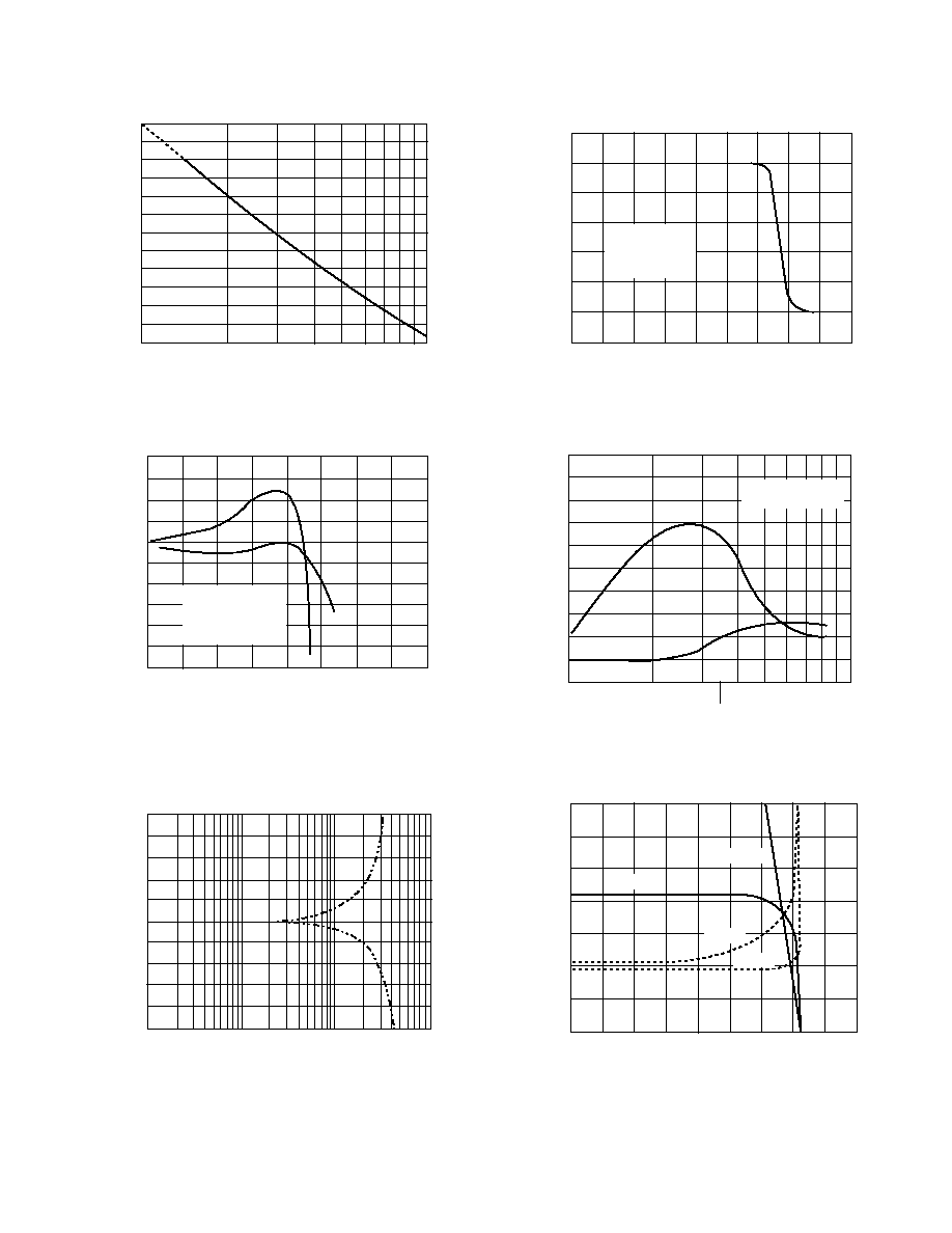
The test circuit of Figure 7 allows two DC bias levels, set by
the user, to be superimposed on a high frequency signal
source. A computer controlled relay selects either the preset
blanking or luminance level. One measurement is taken at
each level and the change in gain or phase is calculated.
This procedure is repeated one hundred times to provide a
reasonably large sample.
DIFFERENTIAL GAIN AND PHASE TEST CIRCUIT
Fig. 7 Differential Phase and Gain Test Circuit
Fig. 5 Chip Disabled Crosstalk Test Circuit
V
OUT
37.5
ENABLED
CROSSPOINT
V
IN
V
IN
V
OUT
R
IN
All hostile crosstalk = 20 log
V
OUT
V
IN
Chip disabled crosstalk = 20 log
V
IN
V
OUT
75
AC
COUPLING
x 2
BUFFER
AMP
3.9 k
8 V
10
µ
H
10
µ
H
LUMINANCE LEVEL
BLANKING LEVEL
220
RELAY SWITCH
0.1
µ
F
R
L
C
L
75
150
150
75
R.F. SIGNAL
SOURCE
R
L
10 k
The results are averaged to reduce the standard deviation
and therefore improve the accuracy of the measurement.
The output from the device under test is AC coupled to a
buffer amplifier which allows the buffer to operate at a
constant luminance level so that it does not contribute any dg
or dp to the measurement.
CONTROL BIT
FROM
I
/O PORT
DUT
0.5
µ
s/div
1
µ
s/div
Fig. 4 Switching Envelope (crosspoint to crosspoint)
Fig.3
Switching Transient (crosspoint to crosspoint)
Fig. 6 All Hostile Crosstalk Test Circuit
10 mV/div
0.1 V/div

510 -34 -2
7
OPTIMISING THE PERFORMANCE OF THE GX434
1.
Power Supply Considerations
Table 1 shows the effect on differential gain (dg) and
differential phase (dp) of various power supply voltages
that may be used. A nominal supply voltage of
±
8
volts result in parameter values as shown in the top
row of the table. By using other power supply voltage
combinations, improvements to these parameters are
possible at the sacrifice of increased chip power
dissipation. Maximum degradation of the differential
gain and phase occurs for the last combination of +12
, -7 volts along with an increase in power dissipation;
these voltages are not recommended.
Table 2 shows the general characteristic variations
of the GX434 when different combinations of power
supply voltages are used. These changes are rela-
tive to a circuit using
±
8 volts Vcc.
Supply Voltage
Characteristic Changes
±
7
- lower logic thresholds
- max logic I/P (
4.5V)
- loss of off isolation (
20 dB)
- poorer dg and dp
+8/ -12
- slight increase in negative
supply current
- slight decrease in offset
- very similar frequency response
- better dg and dp
±
12
- increase in supply current (10%)
- increase in offset (
2-4 mV)
- very similar frequency response
- better dg and dp
+12/ -7
- loss in off isolation (
20 dB)
- poorer dg and dp
Supply
Differential Gain
Differential Phase
Voltage
%
degrees
(Typical)
(Typical)
±
8
0.030
0.012
+8/ -12
0.010
0.007
±
12
0.010
0.007
+12/ -7
0.084
0.080
The GX434 does not require input DC biasing to
optimise dg or dp nor does it need switching
transient suppression at the output. Furthermore,
both the analog signal and logic circuits within the
chip use one common power supply, making power
supply configurations relatively simple and straight-
forward. Several of the input characteristic graphs
on pages 4-5 show that for best operation, the input
bias should be 0 volts. The switching transient
photographs on page 6 show how small the actual
transients are and clearly show the make-before-
break action of the GX434 video multiplexer switch.
510 -34 -2
8
3. Multi-chip Considerations
Whenever multi-chip bus systems are to be used, the total
input and output capacitance must be carefully considered.
The input capacitance of an enabled crosspoint (chip selected),
is typically only 2 pF and increases slightly to 2.4 pF when the
chip is disabled. The total output capacitance when the chip
is disabled is approximately 15 pF per chip.
Usually the GX434 multiplexer switch is used in a matrix
configuration of (n x 1) crosspoints perhaps combined in an
(n x m) total routing matrix. This means for example, that four
ICs produce a 16 x 1 configuration and have a total output
capacitance of 4 x15 pF or 60 pF if all four chips are disabled.
For any one enabled crosspoint, the effective load capacitance
will be 3 x15 pF or 45 pF.
In a multi-input/multi-output matrix, it is important to consider
the total input bus capacitance. The higher the bus capacitance
and the more it varies from the ON to OFF condition, the more
difficult it is to maintain a wide frequency response and
constant drive from the input buffer. A 16 x 16 matrix using 64
ICs (16 x 4), would have a total input bus capacitance of 16 x
2.4 pF or 40 pF.
Fig.10 Multi-chip Connections
+8V
A0
A1
CS
OUTPUT
NC
-8V
IN 3
IN 2
GND
GND
IN 1
GND
IN 0
1
2
3
4
5
6
7
14
13
12
11
10
9
8
R
1k
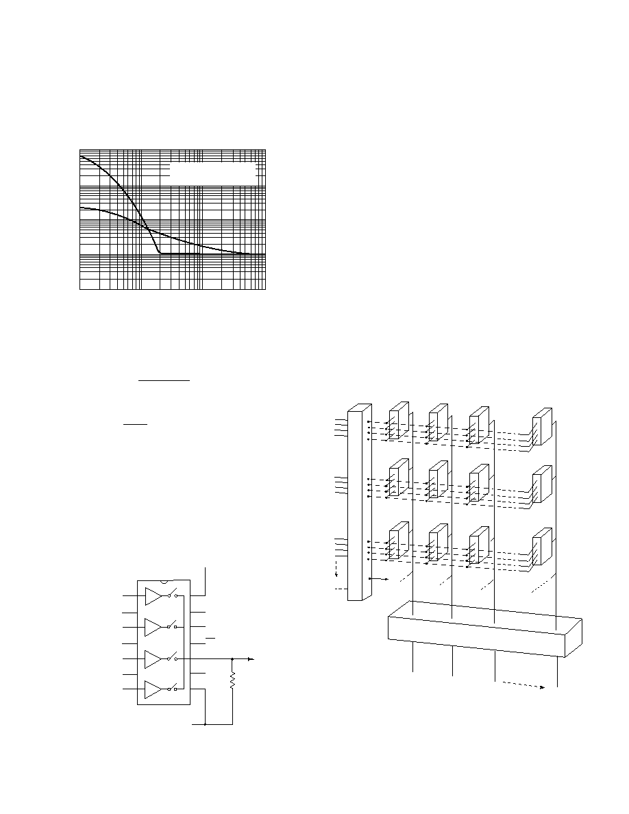
Fig.9 Negative Slew Rate (-SR) Improvement
2.
Load Resistance Considerations
The GX434 crosspoint switch is optimised for load resistances
equal to or greater than 3 k
. Figure 8 shows the effect on the
differential gain and phase when the load resistance is varied
from 100
to 100 k
.
The negative slew rate is dependant upon the output current
and load capacitance as shown below.
-SR =
I
+
3 mA
I
8 mA
The current
I
is
determined from the following equation:
I
= -V
EE
R
1 k
It is possible to increase the negative slew rate (-S.R.) and thus
the large signal bandwidth, by adding a resistance from the
output to - V
EE
. This resistor increases the output current above
the 3 mA provided by the internal current generator and
increases the negative slew rate. The additional slew rate
improving resistance must not be less than 1k
in order to
prevent excessive currents in the output of the device. An
adverse effect of utilising this negative slew rate improving
resistor, is the increase in differential phase from typically
0.009
∞
to 0.014
∞
. Under these same conditions, the differential
gain drops from typically 0.033 % to 0.021 %.
= 3.58 MHz, 20 IRE
BLANKING LEVEL = 0V DC
dp
dg
100
1K
10K
100K
10
1.0
0.1
0.01
0.001
R
L
(
)
Fig. 8
dg/dp
vs R
L
C
L
R
I N P U T B U F F E R S
GX
414
GX
414
GX
414
GX
414
GX
414
GX
414
GX
414
GX
414
GX
414
GX
414
GX
414
GX
414
O U T P U T
B U F F E R S
1
2
3
4
5
6
7
8
9
10
11
12
n
1
2
3
m
DIFFERENTIAL PHASE & GAIN (DEGREES & %)

510 -34 -2
9
BINARY ADDRESS
DECODER
VIDEO INPUTS
GX434 SWITCHES
V 0
V 1
V 2
V 3
75
75
75
75
0.1
1
2
6
5
4
3
7
9
10
11
12
13
14
8
1
2
6
5
4
3
7
9
10
11
12
13
14
8
1
2
6
5
4
3
7
9
10
11
12
13
14
8
1
2
6
5
4
3
7
9
10
11
12
13
14
8
V 4
V 5
V 6
V 7
75
75
75
75
V 8
V 9
V 10
V 11
75
75
75
75
V 12
V 13
V14
V15
75
75
75
75
0.1
0.1
0.1
0.1
0.1
0.1
0.1
-8V
-8V
+8V
-8V
+8V
+8V
A 0
A 1
330
2-10pF
IN 0
IN 1
IN 2
IN 3
+V
A 0
A 1
CS
OUT
-V
IN 0
IN 1
IN 2
IN 3
+V
A 0
A 1
CS
OUT
R
EXT
-V
IN 0
GND
IN 2
IN 3
+V
A 0
A 1
CS
OUT
-V
IN 0
IN 1
IN 2
IN 3
+V
A 0
A 1
CS
OUT
-V
A 2
ENABLE
A 3
4
5
6
7
-8V
+8V
GND
GND
GND
GND
GND
GND
GND
GND
GND
2
3
1
1
2
74HC139
GND
GND
IN 1
+5V
0.1
8
16
33K
1%
33K
1%
33K
1%
33K
1%
R
EXT
R
EXT
R
EXT
APPLICATIONS INFORMATION
The GX434 multiplexer is a very high performance,
wideband circuit requiring careful external circuit design.
Good power supply regulation and decoupling are
necessary to achieve optimum results. The circuit designer
must use proper lead dress, component placement and
PCB layout as in any high frequency circuit.
Functionally, the video switches are non-inverting, unity
gain bipolar switches with buffered inputs requiring DC
coupling and 75
line terminating resistors when directly
driven from 75
cable. The output must be buffered to
drive 75
lines. This is usually accomplished with the
addition of an operational amplifier/ buffer which also
allows adjustments to be made to the gain, offset and
frequency response of the overall circuit.
A typical video routing application is shown in Figure 11.
Four ICs are used in a 16 x 1 multiplexer switching circuit.
An external address decoder is shown which generates
the 16 address and chip enable codes from a binary
number. The address inputs to each chip are active high
while the chip select inputs are active low. Depending on
the application and speed of the logic family used,
latches may be required for synchronization where timing
and delays are critical. Since the individual crosspoint
switching circuits are unidirectional bipolar elements, low
crosstalk and high isolation are inherent. The make-
before-break switching characteristics of the GX434
means virtually 'glitch' free switching.
+5V
0.1
-
+
3
2
4
7
-5V
0.1
75
500
6
250
300
100
Video
Out
All resistors in ohms, all capacitors in
microfarads unless otherwise stated.
Fig.11 16 x 1 Video Multiplexer Circuit
CLC 410 (comlinear)
DOCUMENT
IDENTIFICATION
PRODUCT PROPOSAL
This data has been compiled for market investigation purposes
only, and does not constitute an offer for sale.
ADVANCE INFORMATION NOTE
This product is in development phase and specifications are
subject to change without notice. Gennum reserves the right to
remove the product at any time. Listing the product does not
constitute an offer for sale.
PRELIMINARY DATA SHEET
The product is in a preproduction phase and specifications are
subject to change without notice.
DATA SHEET
The product is in production. Gennum reserves the right to make
changes at any time to improve reliability, function or design, in
order to provide the best product possible.
Gennum Corporation assumes no responsibility for the use of any circuits described herein and makes no representations that they are free from patent infringement.
©Copyright August 1989 Gennum Corporation. Revision date: January 1993. All rights reserved. Printed in Canada.