 | –≠–ª–µ–∫—Ç—Ä–æ–Ω–Ω—ã–π –∫–æ–º–ø–æ–Ω–µ–Ω—Ç: LC506 | –°–∫–∞—á–∞—Ç—å:  PDF PDF  ZIP ZIP |
FEATURES
∑
operating supply voltage 1.1 to 1.55 VDC
∑
40 dB feedback stabilized gain
∑
38 dB gain trim
∑
0.95 regulated voltage LC506
∑
0.90 regulated voltage LV506
2(
2
)
_
+
230
30K
1(
1
)
5(
7
)
6(
8
)
4(
6
)
3(
3
)
REGULATOR
V
REG
V
B
INPUT
OUTPUT
GAIN SET
GND
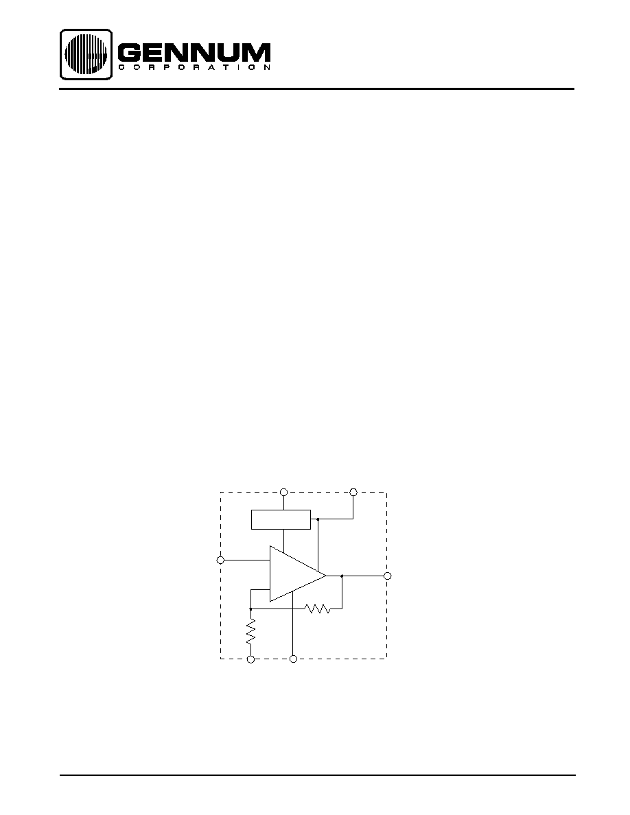
BLOCK DIAGRAM
Linear Class A Preamplifiers
LC506/LV506 DATA SHEET
DESCRIPTION
The LC506 and LV506 are class A non-inverting preamplifiers
with 40 dB feedback controlled, stabilized gain.
Gain trim is provided at pin 1, which simultaneously affects
both gain and output noise, independent of the main volume
control.
A voltage regulator is built on-chip to supply the amplifier and
electret microphone with precision reference voltage. A typical
regulator voltage for the LC506 is 0.95V, while it is 0.90V for the
LV506. This regulator feature of the LC506 allows it to be used
with the high power LD549 to provide increased supply rejection
during transient drops in supply voltage, caused by high
current peaks in the LD549.
Both LC506 and LV 506 devices are capable of operating from
a supply voltage of 1.55 VDC while continuously providing
80 dB of regulator supply rejection.
Bracketed pin-out for LC506
STANDARD PACKAGING
∑
8 pin MICROpac (LC506)
∑
8 pin MINIpac (LC506)
∑
8 pin PLID
Æ
(LC506)
∑
6 pin MINIpac (LV506)
Revision Date: January 1996
GENNUM CORPORATION P.O. Box 489, Stn A, Burlington, Ontario, Canada L7R 3Y3 tel. (905) 632-2996 fax: (905) 632-5946
Japan Branch: A-302, M i yamae Vi l l age, 2≠10≠42 M i yamae, Suginami≠ku Tokyo 168, Japan tel. (03) 3334-7700 fax (03) 3247-8839
Document No. 500 - 26 - 05
500 - 26 - 05
2
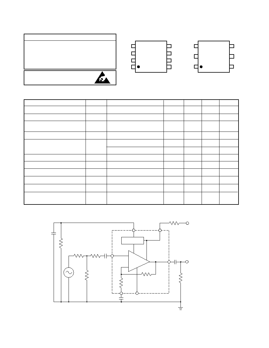
ELECTRICAL CHARACTERISTICS
Conditions : V
B
= 1.30 VDC
, temperature 25∞C
2(2)
230
30K
1(1)
5(7)
6(8)
4(6)
3(3)
V
B
=1.3 VDC
0.1
V
OUT
47
10
10 K
+
0.1
3.3 K
4.7 K
33 K
+
10
V
IN
1 kHz
R
B
=4.7
REGULATOR
_
+
PARAMETER SYMBOL CONDITIONS
MIN
TYP MAX UNITS
Gain A
V
V
OUT
= 0.25V
RMS (Note 1)
Temperature Coefficient of Gain
Quiescent Current (incl. microphone
simulator circuit)
Temperature Coefficient of Current
Microphone Supply Voltage
LC506
LV506
Input Referred Noise
Total Harmonic Distortion and Noise
V
OUT
= 0.25 V
RMS
Maximum Output at 7% THD
Input Impedance
Output Impedance
Frequency Response High (-3dB)
Low (-3dB)
PARAMETER
VALUE / UNITS
Supply Voltage
3 VDC
Power Dissipation 60 mW
Storage Temperature -20 to + 70
∞
C
Operating Temperature
-10 to + 60
∞
C
ABSOLUTE MAXIMUM RATINGS
PIN CONNECTION
1
4
5
8
8 PIN
1
3
4
6
I / P
GND
6 PIN
38
-
182
-
0.90
0.85
-
-
-
-
-
-
-
41
0.03
300
44
-
362
dB
dB/∞C
µ
A
-2.0
0.95
0.90
1.2
1.5
350
30
2.5
5
0.2
-
1.00
0.95
2.0
3.8
-
-
-
-
-
µ
A/∞C
V
V
µ
V
%
mV
RMS
k
k
kHz
kHz
CAUTION
CLASS 1 ESD SENSITIVITY
I/P
N/C
V
REG
V
REG
Gain
Set
V
B
O/P
Gain
Set
Microphone Simulator Circuit
Bracketed pin-out for LC506
All external resistors in ohms, all capacitors in
µ
F unless otherwise stated
Fig. 1 Test Circuit
Note 1:
A
V
= 20 log (VOUT/ V
IN
) + 40 dB where 40 dB is input attenuator
All parameters and switches remain as shown in test circuit unless stated in conditions column.
GND
V
B
N/C
O/P
500 - 26 - 05
3
10k
1k
100
30
40
50
1k
100
10k
20
0
40
60
R
GT
(
)
Frequency (Hz)
1.1
38
40
1.0
1.2
1.3
1.4
1.5
V
B
(V)
39
41
60
40
20
10
0
-20
T
A
(
o
C)
-20
0
20
40
T
A
(
o
C)
0.8
60
1.2
1.0
-20
0
20
40
T
A
(
o
C)
250
350
450
60
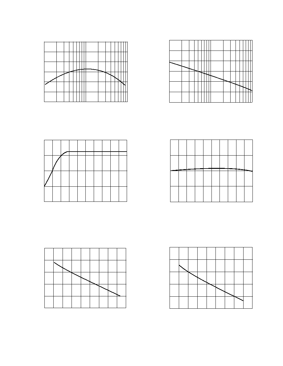
Fig. 2
Frequency Response
Fig.3
Gain vs Gain Trim Resistor
Fig. 4 Voltage Gain vs Battery Voltage
Fig. 5 Gain vs Temperature
Fig. 7 Quiescent Current vs Temperature
Fig. 6 Regulating Voltage vs Temperature
DEVICE CHARACTERISTICS
GAIN (dB)
GAIN (dB)
GAIN (dB)
GAIN (dB)
REGULATING VOLTAGE (V)
QUIESCENT CURRENT (
µ
A)
500 - 26 - 05
4
2
470
TYP
0.047
1
5
6
4
3
V
B
=1.3 VDC
6.8
N/C
8
0.1
6.8
2.2
6.8
7
LC/LD549
R
GT
10K
0.01
2
1
5
6
4
3
R
VC
=10K
LC506
+
MIC
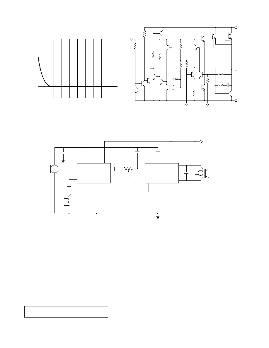
Fig. 10 Typical Application Circuit
All resistors in ohms, all capacitors in
µ
F unless otherwise stated
Fig. 9 Equivalent Circuit
All Resistors in ohms, all capacitors in
µ
F unless otherwise stated
Note :
Use LD549 with LV506
V
B
(V)
250
350
450
1.1
1.0
1.2
1.3
1.4
1.5
Fig. 8 Quiescent Current vs Battery Voltage
OUTPUT
GROUND
230
30K
V
REG
INPUT
V
B
30K
GAIN TRIM
Gennum Corporation assumes no responsibility for the use of any circuits described herein and makes no representations that they are free from patent infringement.
© Copyright Sept. 1982 Gennum Corporation. Revision Date: November 1991 All rights reserved. Printed in Canada.
REVISION NOTES
Chip information removed.
QUIESCENT CURRENT (
µ
A)