 | –≠–ª–µ–∫—Ç—Ä–æ–Ω–Ω—ã–π –∫–æ–º–ø–æ–Ω–µ–Ω—Ç: LC550 | –°–∫–∞—á–∞—Ç—å:  PDF PDF  ZIP ZIP |

40 dB
OUT B2
IN B
OUT B1
DEC B2
V
B
GND
OUT A
IN A
2.2k
V
MIC
1
2
4
3
5
10
9
7
6
23 dB
DEC B1
8
DESCRIPTION
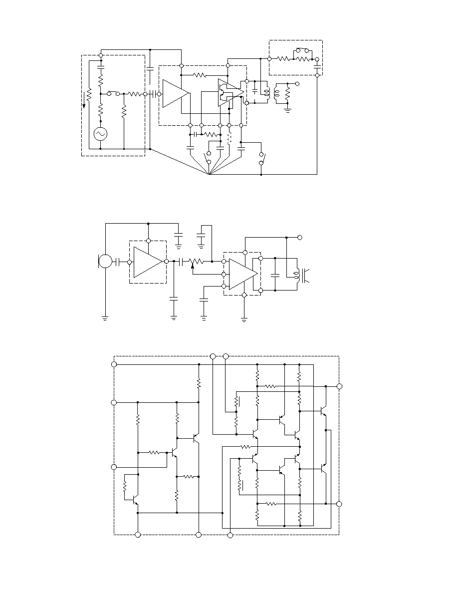
The LC550 is a low voltage linear monolithic integrated
circuit amplifier. It is comprised of two separate amplifiers
on a single chip. The first is a 23 dB Class A preamp
followed by a 40 dB Class B output stage.
Both stages incorporate negative feedback to control
gain, minimize distortion and stabilize operation at very
low quiescent currents.
The preamp and output stage have their inputs and outputs
separately pinned out. This is an advantage as it allows
access to both stages, providing the designer with flexibility
and a full range volume control.
The combination of low quiescent current and a medium
power push-pull output makes the LC550 suitable for
medium power BTE hearing aids and for high power ITE
aids where efficiency and battery life are a premium
consideration.
FEATURES
Medium Power
Class B Amplifier
∑
23 dB class A preamp & 40 dB class B output stage
∑
1.0 V DC to 1.7 V DC operating range
∑
2.2 k
on chip microphone decoupling resistor
∑
350
µ
A typical quiescent current
∑
400 Hz to 20 kHz frequency response
STANDARD PACKAGING
∑ 10 pin MICROpac
∑ 10 pin MINIpac
∑ 10 pin SLT
∑ 10 pin PLID
Æ
∑ Chip (57 x 47 mils)
Au Bump
BLOCK DIAGRAM
All resistors in ohms, all capacitors in
µ
F unless otherwise stated.
U.S. Patent No. 4,085,382, patented in other countries.
LC550 DATA SHEET
Document No. 500 - 37 - 8
GENNUM CORPORATION P.O. Box 489, Stn A, Burlington, Ontario, Canada L7R 3Y3 tel. (905) 632-2996 fax: (905) 632-5946
Japan Branch: A-302, M i yamae Vi l l age, 2≠10≠42 M i yamae, Suginami≠ku, Tokyo 168, Japan tel. (03) 3334-7700 fax (03) 3247-8839
Revision Date: December 1994

2
500 - 37 - 8
PARAMETER
VALUE/UNITS
Supply Voltage
3 V
Power Dissipation
60 mW
Operating Temperature Range
-10
∞
C to 60
∞
C
Storage Temperature Range
-20
∞
C to 70
∞
C
ABSOLUTE MAXIMUM RATINGS
TOP VIEW
PIN CONNECTION
CAUTION
CLASS 1 ESD SENSITIVITY
5
10
1
6
V
MIC
OUT A
IN A
V
B
GND
OUT B2
DEC B2
IN B
OUT B1
Gain
A
V
Output Level 0.707 V
RMS
59
63
67
dB
Total Current (including
I
MIC
)
I
TOT
S1 - open
-
350
475
µ
A
Input Referred Noise
IRN
NFB 0.2 to 10kHz at 12dB/Oct
-
1.5
3
µ
V
Total Harmonic Distortion
THD
Output Level 0.707 V
RMS
-
3.5
7.5
%
O/P Swing at 7% Distortion
-
1.4
-
V
RMS
Stable with Battery Resistance to:
S4 - open
-
-
60
Preamp O/P Impedance
-
1.1
-
k
Preamp I/P Impedance
-
30
-
k
O/P Stage O/P Impedance
-
110
-
O/P Stage I/P Impedance
18
27
34
k
Start-Up Time
Refer to start up test sequence
-
-
3
sec
PARAMETER
SYMBOL
CONDITIONS
MIN
TYP
MAX
UNITS
Power Supply
Off
S1
Open
Removes V
IN
S2 / S3
Closed
Discharges C2 & C3
S1
Closed
Applies V
IN
(V
IN
level is
determined from Gain Test)
S2 / S3
Open
Removes Short from C2 and C3
Power Supply
On
Gain must be within specification, within 3 seconds after Power Supply is turned on
START-UP TEST SEQUENCE
SEQUENCE CONDITIONS
COMMENT
ELECTRICAL CHARACTERISTICS
All switches remain as shown in Test Circuit
Conditions: Supply voltage V
B
= 1.3 V DC, Temperature ambient = 25
∞
C, Ground line resistance 0.03
max., Volume control setting max. gain
DEC B1
3
500 - 37 - 8
MIC SUPPLY
+
S1
10
7
3
4
C2
2.2
22k
BATTERY
SIMULATOR
5
820
6
2.2k
33K
I
2
8
0.01
MIC
+
9
10k
S2
0.047
10
3.3k
1.3 V DC
1
V11
1kHz
V1
220
C3
2.2
S3
S4
RB
I
TOT
4.7
VB
VO
1k
0.047
40dB
23dB
RG*
+
4.7
0.022
NOTES:
1. 42.13 dB of attenuation from V1 to V11
2 *RG (equivalent gnd resistance) should not exceed 30 m
(increasing RG increases distortion)
All resistors in ohms, all capacitors in
µ
F unless otherwise stated.
MICROPHONE SIMULATOR
Fig. 1 Test Circuit
2k TYP
0.047
10k
7
3
4
2.2
5
0.022
6
2
8
+
9
10
0.01
1.3 V DC
1
2.2
V
B
40dB
4.7
NOTE1
0.047
23dB
+
+
NOTE:
1. 2.2
µ
F when receiver is
3k
All resistors in ohms, all capacitors in
µ
F unless otherwise stated.
Fig. 2 Typical Hearing Aid Application
33k
4
5
27k
2.2k
2
1
3
8
9
10
6
7
All resistors in ohms, all capacitors in
µ
F unless otherwise stated.
U.S. Patent No. 4,085,382, patented in other countries.
Fig.3 Functional Schematic
4
500 - 37 - 8
0
0.1
0.2
0.3
0.4
0.5
0.6
0.7
RELATIVE VOLTAGE GAIN (dB)
0 20 40 60 80 100
BATTERY RESISTANCE (
)
35
30
25
20
15
10
5
0
DISTORTION ( % )
0 20 4 0 60 80 100
GROUND RESISTANCE ( m
)
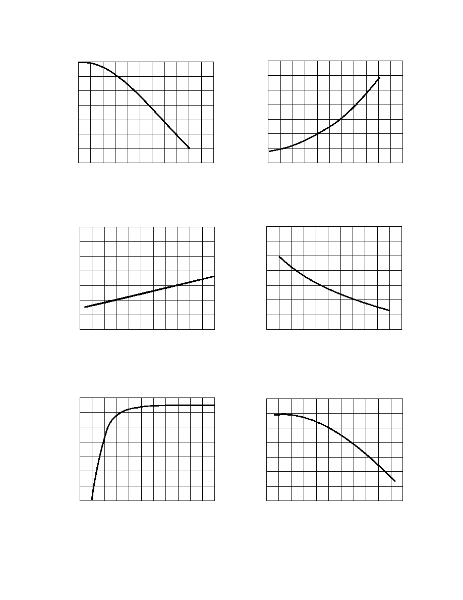
Fig. 5 Distortion vs Ground Line Resistance
Fig. 4 Gain vs Battery Resistance
700
600
500
400
300
200
100
0
825
725
625
525
425
325
225
125
0.6
0.8
1.0
1.2 1.4 1.6
SUPPLY VOLTAGE (V)
-40
-20 0 20 40 60
TEMPERATURE (
o
C)
70
60
50
40
30
20
10
0
GAIN (dB)
0.6 0.8 1.0 1.2 1.4 1.6
SUPPLY VOLTAGE (V)
70
68
66
64
62
60
58
56
GAIN (dB)
-40 -20 0 20 40 60
TEMPERATURE (
o
C)
Fig. 9 Gain vs Temperature
Fig. 8 Gain vs Supply Voltage
TOTAL CURRENT (
µ
A)
TOTAL CURRENT (
µ
A) (with S1 open)
Fig. 6 Total Current vs Supply Voltage
Fig. 7 Total Current vs Temperature
5
500 - 37 - 8
DOCUMENT
IDENTIFICATION
PRODUCT PROPOSAL
This data has been compiled for market investigation purposes
only, and does not constitute an offer for sale.
ADVANCE INFORMATION NOTE
This product is in development phase and specifications are
subject to change without notice. Gennum reserves the right to
remove the product at any time. Listing the product does not
constitute an offer for sale.
PRELIMINARY DATA SHEET
The product is in a preproduction phase and specifications are
subject to change without notice.
DATA SHEET
The product is in production. Gennum reserves the right to make
changes at any time to improve reliability, function or design, in
order to provide the best product possible.
100
1k
10k 100k
LOAD IMPEDANCE (
)
10 100 1k 10k 100k
FREQUENCY (Hz)
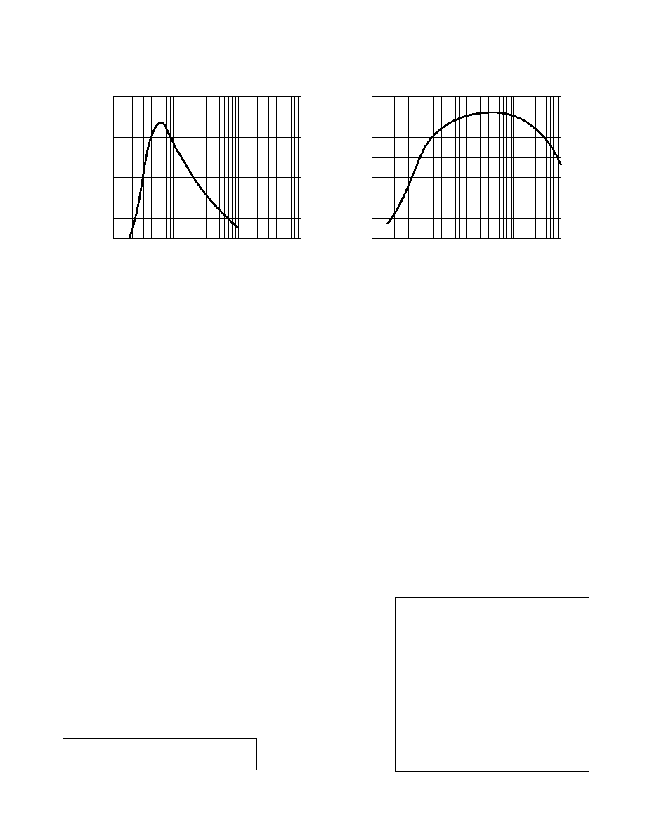
POWER (mW)
3.5
3.0
2.5
2.0
1.5
1.0
0.5
0
Fig. 10 Power Output vs Load Impedance
at 7% Distortion
10
0
-10
-20
-30
-40
-50
-60
VOLTAGE GAIN (dB)
Fig. 11 Voltage Gain vs Frequency
Gennum Corporation assumes no responsibility for the use of any circuits described herein and makes no representations that they are free from patent infringement.
© Copyright September 1981 Gennum Corporation. All rights reserved. Printed in Canada.
REVISION NOTES
Correction to Fig. 1 Pb/Sn Bump removed