REV NO: V.2
DATE: DEC/05/2002
PAGE: 1 OF4
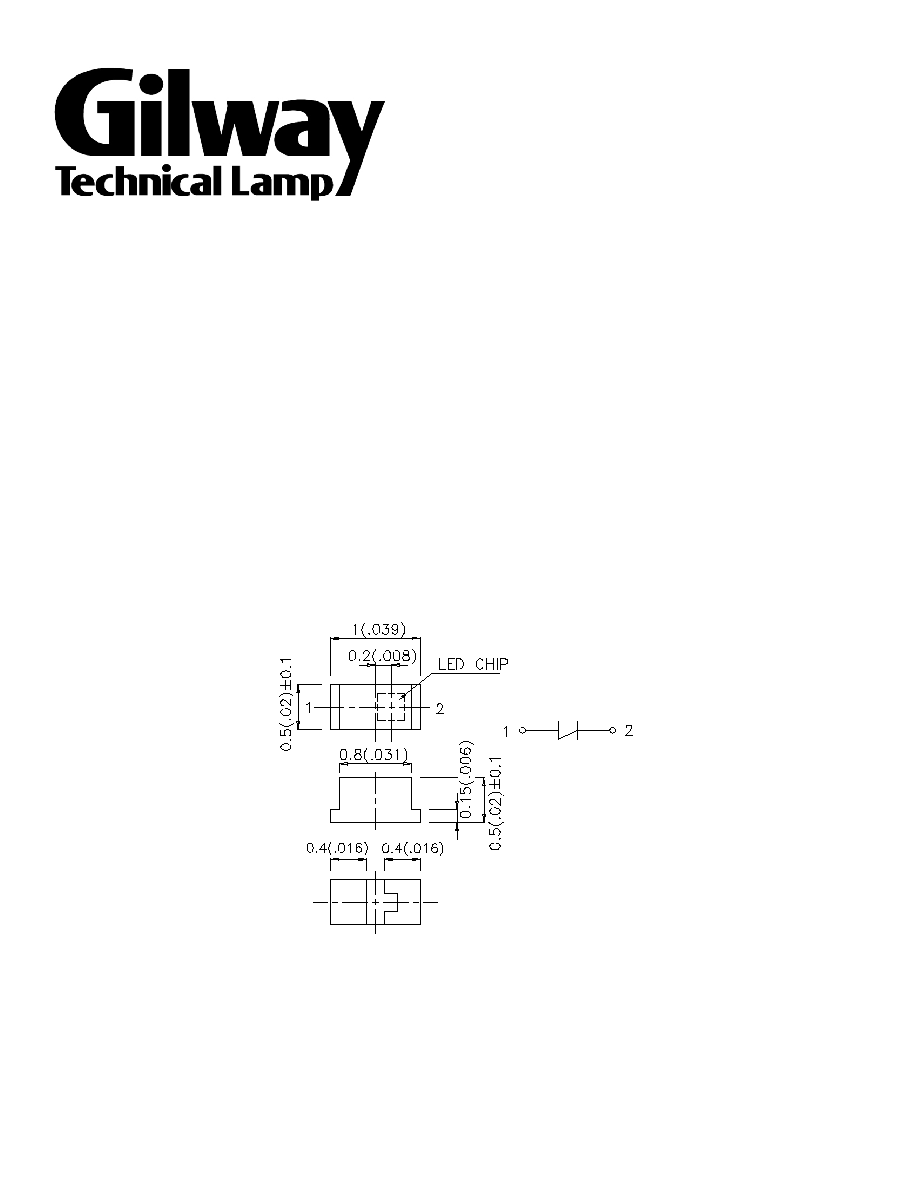
1.0x0.5mm SMD CHIP LED LAMP
Notes:
1. All dimensions are in millimeters (inches).
2. Tolerance is 0.1(0.004") unless otherwise noted.
3. Specifications are subject to change without notice.
Features
!
1.0mmx0.5mm SMT LED, 0.5mm THICKNESS.
!
LOW POWER CONSUMPTION.
!
WIDE VIEWING ANGLE.
!
IDEAL FOR BACKLIGHT AND INDICATOR.
!
VARIOUS COLORS AND LENS TYPES AVAILABLE.
!
PACKAGE : 2000PCS / REEL.
Package Dimensions
Description
The Hyper Red source color devices are made
with DH InGaAlP on GaAs substrate Light Emitting
Diode.
55 Commerce Way
Woburn, MA 01801
(781) 935 - 4442
(781) 938 - 5867
www.gilway.com
GHB-0402-R

REV NO: V.2
DATE: DEC/05/2002
PAGE: 2 OF4
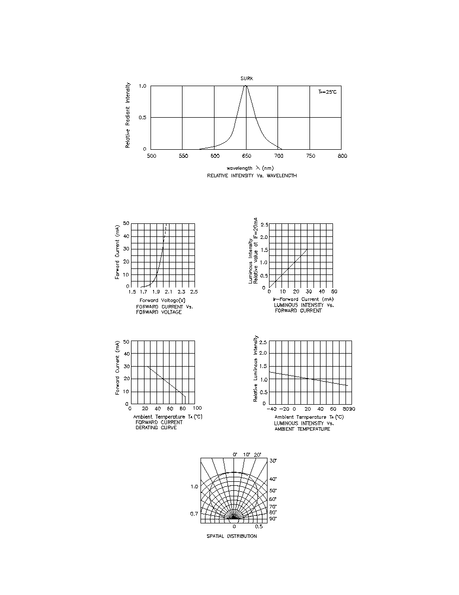
Electrical / Optical Characteristics at T
A
=25 C
Absolute Maximum Ratings at T
A
=25 C
Note:
1. 1/10 Duty Cycle, 0.1ms Pulse Width.
Selection Guide
Note:
1. 1/2 is the angle from optical centerline where the luminous intensity is 1/2 the optical centerline value.
art No.
P
.
P
Pa
a
arrrttt N
N
No
o
o..
P
.
art No
P
e
ic
D e
D
Diiic
c
ce
e
D e
ic
D
e
ens Typ
L
e
L
Le
e
en
n
ns
s
s T
T
Ty
y
y p
p
pe
e
L
e
v (mcd)
Lens Typ
I
)
I
Iv
v
v (((m
m
mc
c
cd
d
d))
I
)
Iv (mcd
iewing
@ 20 mA
V
g
V
Viiie
e
ew
w
w iiin
n
ng
g
V
g
Viewin
Angle
in.
M .
M
Miiin
n
n..
M .
in
M
.
yp
T
.
T
Ty
y
yp
p
p..
T
.
Typ
)
YPERRED( InGaAlP
H
R
ATER CLEA
W
�
120
ymbol
S
l
S
Sy
y
y m
m
mb
b
bo
o
oll
S
l
ymbo
S
r
aramete
P
r
P
Pa
a
arrra
a
am
m
me
e
ettte
e
err
P
r
aramete
P
e
evic
D
e
D
De
e
ev
v
viiic
c
ce
e
D
e
evic
D
.
yp
T
.
T
Ty
y
yp
p
p..
T
.
yp
T
.
ax
M
.
M
Ma
a
ax
x
x ..
M
.
ax
M
s
nit
U
s
U
Un
n
niiittts
s
U
s
nit
U
s
est Conditio n
T
s
T
Te
e
es
s
s ttt C
C
Co
o
on
n
nd
d
diiitttiiio
o
on
n
ns
s
T
s
Test Conditio n
peak
eak Wavelength
P
d
yper Re
H
m
n
I
F
=20mA
D
ominate Wavelength
D
d
yper Re
H
m
n
I
F
=20mA
1/2
pectral Line Half-width
S
d
yper Re
H
m
n
I
F
=20mA
C
e
apacitanc
C
d
yper Re
H
F
p
V
F
=
z
0V;f=1MH
V
F
orward Voltage
F
d
yper Re
H
9
.
1
5
.
2
V
I
F
=20mA
I
R
everse Current
R
d
yper Re
H
0
1
A
u
V
R
= 5V
arameter
P
r
P
Pa
a
arrra
a
am
m
me
e
ettte
e
err
P
r
Paramet e
yper Red
H
d
H
Hy
y
y p
p
pe
e
errr R
R
Re
e
ed
d
H
d
yper Re
H
s
nit
U
s
U
Un
n
niiittts
s
U
s
Unit
Power dissipation
70
1
W
m
DC Forward Current
0
3
A
m
Peak Forward Current [1]
85
1
A
m
Reverse Voltage
5
V
Operating/Storage Temperature
-40 C To +85 C
GHB-0402-R
50
140
5
35
28
635
650

REV NO: V.2
DATE: DEC/05/2002
PAGE: 4 OF4
Recommended Soldering Pattern
(Units : mm)
Tape Specifications
(Units : mm)
SMT Reflow Soldering Instructions
Number of reflow process shall be less than 2 times and cooling
process to normal temperature is required between first and
second soldering process.