
G -LINK
GLT4160L16
1M X 16 CMOS DYNAMIC RAM WITH EXTENDED DATA OUTPUT
Apr 2003 (Rev.4.1)
G-Link Technology Corporation,Taiwan
Web : www.glink.com.tw Email : sales@glink.com.tw
TEL : 886-2-26599658
- 1 -
Features :
Description :
1,048,576
words by 16 bits organization.
Fast access time and cycle time.
Dual
CAS
Input.
Low power dissipation.
Read-Modify-Write,
RAS
-Only Refresh,
CAS
-Before-
RAS
Refresh, Hidden
Refresh and Test Mode Capability.
1024 refresh cycles per 16ms.
Available in 400 mil SOJ / TSOPII
Packages.
Single 3.3V
±
0.3V Power Supply.
All inputs and Outputs are TTL
compatible.
Extended Data-Out(EDO) Page Mode
operation.
Self ≠ refresh capability. (S-Version).
Extended Temperature Available
( -25
∞
C ~ 85
∞
C )
The GLT4160L16 is a 1,048,576 x 16 bit
high-performance CMOS dynamic random
access memory. The GLT4160L16 offers
Fast Page mode with Extended Data Output,
and has both BYTE WRITE and WORD
WRITE access cycles via two
CAS
pins. The
GLT4160L16 has symmetric address and
accepts 1024-cycle refresh in 16ms interval.
All inputs are TTL compatible. EDO
Page Mode operation allows random access
up to 1024 x 16 bits within a page, with cycle
times as short as 18ns.
The GLT4160L16 is best suited for
graphics, and DSP applications requiring
high performance memories.
HIGH PERFORMANCE
45
50
60
70
Max.
RAS
Access Time, (t
RAC
)
45 ns
50 ns
60 ns
70 ns
Max. Column Address Access Time, (t
CAA
)
22 ns
25 ns
30 ns
35 ns
Min. Extended Data Out Page Mode Cycle Time, (t
PC
)
18 ns
20 ns
25 ns
30 ns
Min. Read/Write Cycle Time, (t
RC
)
80 ns
85 ns
104 ns
124 ns
Max.
CAS
Access Time (t
CAC
)
12 ns
14 ns
15 ns
20 ns

G -LINK
GLT4160L16
1M X 16 CMOS DYNAMIC RAM WITH EXTENDED DATA OUTPUT
Apr 2003 (Rev.4.1)
G-Link Technology Corporation,Taiwan
Web : www.glink.com.tw Email : sales@glink.com.tw
TEL : 886-2-26599658
- 2 -
Pin Configuration :
Vcc
DQ
0
A0
A1
1
2
3
4
5
6
7
9
10
11
12
13
NC
OE
LCAS
V
SS
DQ
15
DQ
1
WE
RAS
NC
A
9
A
8
8
14
15
16
17
18
19
20
23
24
25
26
27
28
29
30
31
32
33
34
35
36
37
38
39
40
41
42
DQ
2
DQ
3
Vcc
DQ
4
DQ
5
DQ
6
DQ
7
NC
A2
DQ
14
DQ
13
DQ
12
V
SS
DQ
11
DQ
10
DQ
9
DQ
8
UCAS
A
7
A
6
A
5
GLT416016
SOJ Top View
V
CC
21
V
SS
22
NC
NC
A3
A
4
Vcc
DQ
0
A0
A1
1
2
3
4
5
6
7
9
10
12
13
14
NC
OE
LCAS
V
SS
DQ
15
DQ
1
WE
RAS
NC
A
9
A
8
8
15
16
17
18
19
20
21
24
25
26
27
28
29
30
31
32
33
35
36
37
38
39
40
41
42
43
44
DQ
2
DQ
3
Vcc
DQ
4
DQ
5
DQ
6
DQ
7
NC
A2
DQ
14
DQ
13
DQ
12
V
SS
DQ
11
DQ
10
DQ
9
DQ
8
UCAS
A
7
A
6
A
5
TSOP(Type II)
Top View
V
CC
22
23
V
SS
34
11
NC
NC
NC
A3
NC
A
4
Pin Descriptions:
Name
Function
A
0
- A
9
Address Inputs
RAS
Row Address Strobe
UCAS
Column Address Strobe/Upper Byte Control
LCAS
Column Address Strobe/Lower Byte Control
WE
Write Enable
OE
Output Enable
DQ
0
- DQ
15
Data Inputs / Outputs
V
CC
+3.3V Power Supply
V
SS
Ground
NC
No Connection
G -LINK
GLT4160L16
1M X 16 CMOS DYNAMIC RAM WITH EXTENDED DATA OUTPUT
Apr 2003 (Rev.4.1)
G-Link Technology Corporation,Taiwan
Web : www.glink.com.tw Email : sales@glink.com.tw
TEL : 886-2-26599658
- 3 -
Absolute Maximum Ratings*
Capacitance*
T
A
=25
∞
C, V
CC
=3.3V
±
0.3V, V
SS
=0V
Symbol Parameter
Max.
Unit
C
IN1
Address Input
5
pF
C
IN2
RAS
,
LCAS
,
UCAS
,
WE
,
OE
7
pF
Operating Temperature, T
A
(ambient)
........................................0
∞
C to +70
∞
C
............................(extended)..≠25
∞
C to +85
∞
C
Storage Temperature(plastic).....-55
∞
C to +150
∞
C
Voltage Relative to V
SS
................-1.0V to + 4.6V
Short Circuit Output Current.......................50mA
Power Dissipation.......................................1.0W
C
OUT
Data Input/Output
7
pF
*Note:Operation above Absolute Maximum Ratings can
abversely affect device reliability.
*Note: Capacitance is sampled and not 100% tested
Electrical Specifications
l
CAS
means
UCAS
and
LCAS
.
l
All voltages are referenced to GND.
l
After power up, wait more than 100
µ
s and then, execute eight
CAS
-before-
RAS
or
RAS
-only
refresh cycles as dummy cycles to initialize internal circuit.
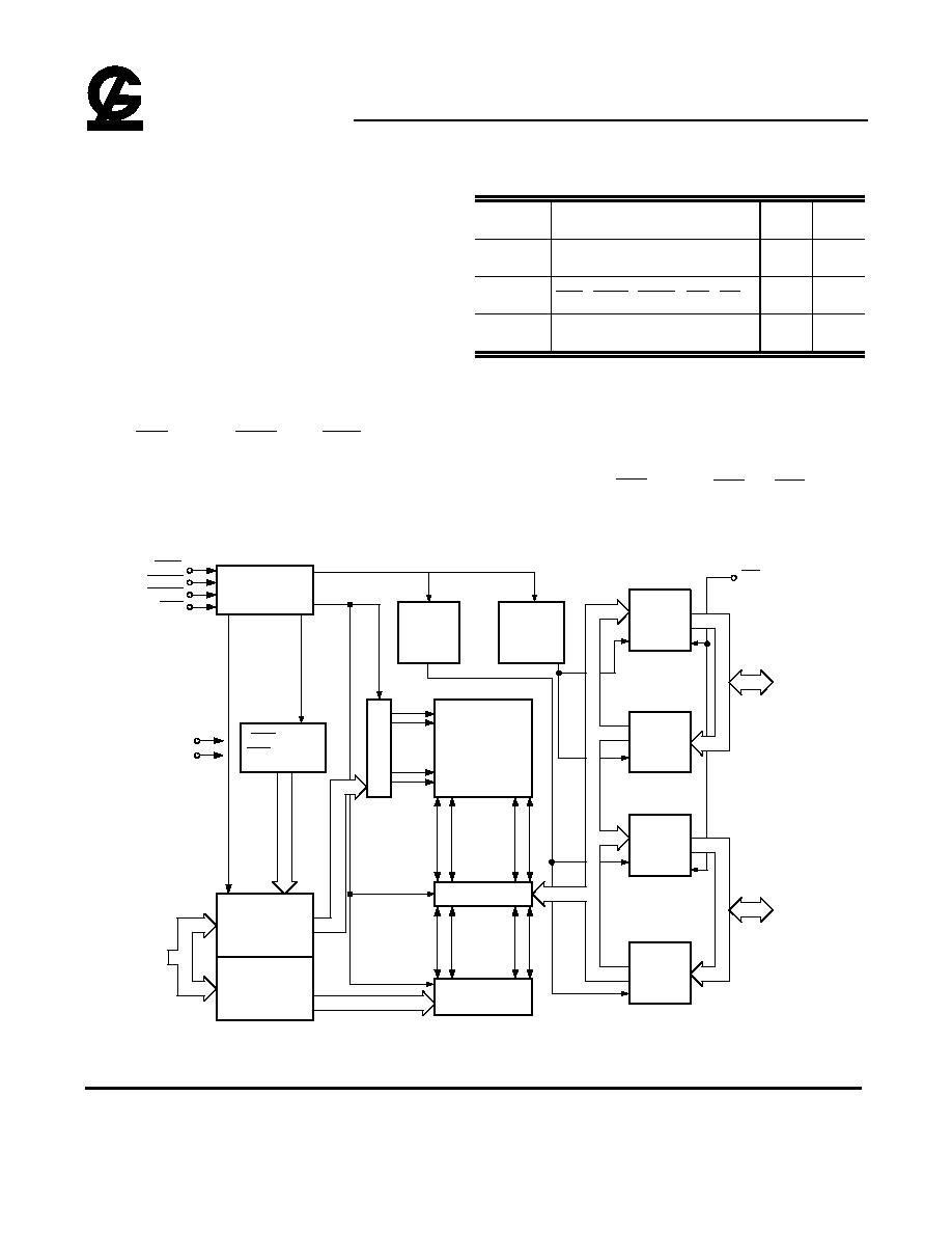
Block Diagram :
Memory
Array
1024X1024X16
Upper
Byte
Control
Sense Amplifier
Column Decoder
Row
Address
Buffer
Column
Address
Buffer
...1024X16...
...1024...
....1024....
Lower
Byte
Control
Row Decoder
Data
Output
Buffer
Data
Input
Buffer
Data
Output
Buffer
Data
Input
Buffer
CAS before
RAS Counter
Clock
Generator
A0
|
A9
X0..X9
Y0..Y9
DQ8
|
DQ15
DQ0
|
DQ7
RAS
LCAS
UCAS
WE
Vcc
GND
OE
X8
X8
X8
X8
X8
X1
6
X8
X8
X8
G -LINK
GLT4160L16
1M X 16 CMOS DYNAMIC RAM WITH EXTENDED DATA OUTPUT
Apr 2003 (Rev.4.1)
G-Link Technology Corporation,Taiwan
Web : www.glink.com.tw Email : sales@glink.com.tw
TEL : 886-2-26599658
- 4 -
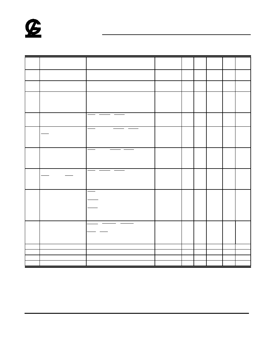
DC and Operating Characteristics (1-2)
T
A
= 0
∞
C to 70
∞
C,-25
∞
C to 85
∞
C (extended temperature) V
CC
=3.3V
±
0.3V, V
SS
=0V, unless otherwise specified.
Sym.
Parameter
Test Conditions
Access
Time
Min. Typ Max. Unit Notes
I
LI
Input Leakage Current
(any input pin)
0V
V
IN
Vcc+0.3V
(All other pins not under test=0V)
-5
+5
µ
A
I
LO
Output Leakage Current
(for High-Z State)
0V
V
out
Vcc
Output is disabled (Hiz)
-5
+5
µ
A
I
CC1
Operating Current,
Random READ/WRITE
t
RC
= t
RC
(min.)
t
RAC
= 45ns
t
RAC
= 50ns
t
RAC
= 60ns
t
RAC
= 70ns
150
150
140
130
mA
1,2
I
CC2
Standby Current,(TTL)
RAS , UCAS , LCAS at V
IH
other inputs
V
SS
1
mA
I
CC3
Refresh Current,
RAS -Only
RAS cycling, UCAS , LCAS at V
IH
t
RC
= t
RC
(min.)
t
RAC
= 45ns
t
RAC
= 50ns
t
RAC
= 60ns
t
RAC
= 70ns
150
150
140
130
mA
2
I
CC4
Operating Current,
EDO Page Mode
RAS at V
IL
, UCAS , LCAS address
cycling:t
PC
=t
PC
(min.)
t
RAC
= 45ns
t
RAC
= 50ns
t
RAC
= 60ns
t
RAC
= 70ns
150
150
140
130
mA
1,2
I
CC5
Refresh Current,
CAS Before RAS
RAS , UCAS , LCAS
address cycling:
t
RC
=t
RC
(min.)
t
RAC
= 45ns
t
RAC
= 50ns
t
RAC
= 60ns
t
RAC
= 70ns
150
150
140
130
mA
1
I
CC6
Standby Current,
(CMOS)
RAS
V
CC
-0.2V,
UCAS
V
CC
-0.2V,
LCAS
V
CC
-0.2V,
All other inputs V
SS
300
µ
A
1,5
I
CC7
Self Refresh Current
RAS = UCAS = LCAS =V
IL
WE = OE =A
0
~A
9
=V
CC
-0.2V or 0.2V
DQ
0
~DQ
15
=V
CC
-0.2V,0.2V or Open
300
µ
A
V
IL
Input Low Voltage
-0.3
+0.8
V
3
V
IH
Input High Voltage
2.0
V
CC
+0.3
V
3
V
OL
Output Low Voltage
I
OL
= 2mA
0.4
V
V
OH
Output High Voltage
I
OH
= -2mA
2.4
V
Notes:
1.I
CC
is dependent on output loading when the device output is selected. Specified I
CC
(max.) is measured with the output open.
2.I
CC
is dependent upon the number of address transitions specified I
CC
(max.) is measured with a maximum of one transition per address cycle in
random Read/Write and EDO Fast Page Mode.
3.Specified V
IL
(min.) is steady state operation. During transitions V
IL
(min.) may undershoot to -1.0V for a period not to exceed 15ns. All AC
parameters are measured with V
IL
(min.)
V
SS
and V
IH
(max.)
V
CC
.
4.Specified V
IH
(max.) is steady state operation. During transitions V
IH
(max.) may undershoot to +1.0V for a period not to exceed 15ns. All AC
parameters are measured with V
IL
(min.)
V
SS
and V
IH
(max.)
V
CC
.
5.S-Version.
G -LINK
GLT4160L16
1M X 16 CMOS DYNAMIC RAM WITH EXTENDED DATA OUTPUT
Apr 2003 (Rev.4.1)
G-Link Technology Corporation,Taiwan
Web : www.glink.com.tw Email : sales@glink.com.tw
TEL : 886-2-26599658
- 5 -
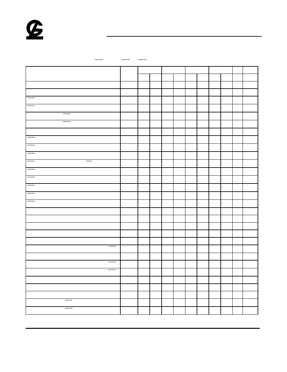
AC Characteristics
T
A
= 0
∞
C to 70
∞
C, -25
∞
C to 85
∞
C (extended temperature),V
CC
= 3V
±
0.3V, V
IH
/ V
IL
= 3.0/0 V, V
OH
/V
OL
= 2.0/0.8V
An initial pause of 100
µ
s and 8
CAS
-before-
RAS
or
RAS
-only refresh cycles are required after power-up.
45
50
60
70
Parameter
Symbol
Min. Max. Min. Max. Min. Max. Min. Max. Unit Notes
Read or Write Cycle Time
t
RC
80
85
104
124
ns
Read Modify Write Cycle Time
t
RWC
103
106
133
170
ns
RAS
Precharge Time
t
RP
30
30
40
50
ns
RAS
Pulse Width
t
RAS
45
100K
50
100K
60
100k
70
10k
ns
Access Time from
RAS
t
RAC
45
50
60
70
ns
1,2,3
Access Time from
CAS
t
CAC
12
14
15
20
ns
1,5,10
Access Time from Column Address
t
AA
22
25
30
35
ns
1,5,6
CAS
to Output Low-Z
t
CLZ
0
0
0
3
ns
CAS
to Output High-Z
t
CEZ
3
8
3
8
3
10
3
20
ns
RAS
Hold Time
t
RSH
13
14
13
20
ns
RAS
Hold Time Referenced to
OE
t
ROH
9
9
10
10
ns
CAS
Hold Time
t
CSH
40
45
40
50
ns
CAS
Pulse Width
t
CAS
7
10K
8
10k
12
10k
15
10k
ns
RAS
to CAS Delay Time
t
RCD
18
33
19
37
18
45
20
50
ns
RAS
to Column Address Delay Time
t
RAD
13
23
14
25
13
30
15
35
ns
7
CAS
to RAS Precharge Time
t
CRP
5
5
5
5
ns
Row Address Set-Up Time
t
ASR
0
0
0
0
ns
Row Address Hold Time
t
RAH
8
9
10
10
ns
Column Address Set-Up Time
t
ASC
0
0
0
0
ns
Column Address Hold Time
t
CAH
6
7
10
15
ns
Column Address to RAS Lead Time
t
RAL
23
25
30
35
ns
Column Address Hold Time Referenced to
RAS
t
AR
39
44
55
50
ns
Read Command Set-Up Time
t
RCS
0
0
0
0
ns
Read Command Hold Time Referenced to
CAS
t
RCH
0
0
0
0
ns
4
Read Command Hold Time Referenced to
RAS
t
RRH
0
0
0
0
ns
4
Write Command Set-Up Time
t
WCS
0
0
0
0
ns
8,9
Write Command Hold Time
t
WCH
6
6
10
15
ns
Write Command Pulse Width
t
WP
6
6
10
15
ns
Write Command to
RAS
Lead Time
t
RWL
12
13
13
30
ns
Write Command to
CAS
Lead Time
t
CWL
12
13
13
15
ns
G -LINK
GLT4160L16
1M X 16 CMOS DYNAMIC RAM WITH EXTENDED DATA OUTPUT
Apr 2003 (Rev.4.1)
G-Link Technology Corporation,Taiwan
Web : www.glink.com.tw Email : sales@glink.com.tw
TEL : 886-2-26599658
- 6 -
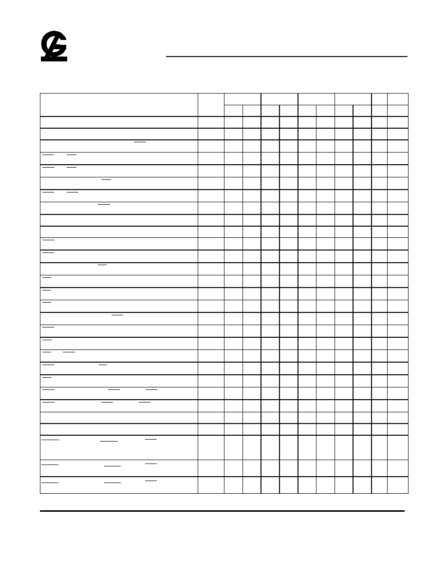
AC Characteristics
45
50
60
70
Parameter
Symbol Min. Max. Min. Max. Min. Max. Min. Max. Unit Notes
Data Set-Up Time
t
DS
0
0
0
0
ns
Data Hold Time
t
DH
8
8
10
15
ns
Data Hold Time Referenced to
RAS
t
DHR
41
46
55
50
ns
RAS
to
WE
E Delay Time
t
RWD
59
64
79
94
ns
CAS
to
WE
Delay Time
t
CWD
24
25
32
44
ns
Column Address to
WE
Delay Time
t
AWD
34
37
47
59
ns
RAS
to
CAS
Precharge Time
t
RPC
0
0
0
0
ns
Access Time from
CAS
Precharge
t
CPA
24
30
32
40
ns
EDO Page Mode Cycle Time
t
PC
18
20
25
30
ns
EDO Page Mode Read-Modify-Write Cycle Time
t
PRWC
52
59
63
71
ns
CAS
Precharge Time (EDO Page Mode)
t
CP
7
8
15
10
ns
RAS
Pulse Width (EDO Page Mode Only)
t
RASP
45
100K
50
100K
60
100k
70
100k
ns
Access Time from
OE
t
OEA
12
14
15
20
ns
OE
to Data Delay Time
t
OED
8
8
13
20
ns
OE
to Output High-Z
t
OEZ
3
8
3
8
3
8
3
20
ns
OE
Command Hold Time
t
OEH
7
7
7
20
ns
Data Output Hold after
CAS
low
t
DOH
5
5
5
5
ns
RAS
to Output High-Z
t
REZ
3
8
3
8
3
8
3
20
ns
WE
to Output High-Z
t
WEZ
3
10
3
12
3
12
3
20
ns
OE
to
CAS
Hold Time
t
OCH
8
8
5
5
ns
CAS
Hold Time to
OE
t
CHO
8
8
5
5
ns
OE
Precharge Time
t
OEP
8
8
5
5
ns
CAS
Set-Up Time for
CAS
-before-
RAS
Cycle
t
CSR
10
10
10
5
ns
CAS
Hold Time for
CAS
-before-
RAS
Cycle
t
CHR
10
10
10
15
ns
Transition Time
t
T
2
50
2
50
2
50
2
50
ns
Refresh Period
t
REF
16
16
16
16
ms
RAS pulse width ( CAS -before-
RAS
Self
refresh)
t
RASS
100
100
100
100
µ
s
RAS precharge time ( CAS -before-
RAS
Self refresh)
t
RPS
80
90
110
130
ns
CAS precharge time ( CAS -before-
RAS
Self refresh)
t
CHS
-50
-50
-50
-50
ns

G -LINK
GLT4160L16
1M X 16 CMOS DYNAMIC RAM WITH EXTENDED DATA OUTPUT
Apr 2003 (Rev.4.1)
G-Link Technology Corporation,Taiwan
Web : www.glink.com.tw Email : sales@glink.com.tw
TEL : 886-2-26599658
- 7 -
Notes:
1. Measure with a load equivalent to one TTL inputs and 50 pF.
2. Assumes that t
RCD
t
RCD
(max.). If t
RCD
is greater than t
RCD
(max.), access time will be t
CAC
dominant.
3. Assumes that t
RAD
t
RAD
(max.). If t
RAD
is greater than t
RAD
(max.), access time will be
controlled by t
AA
.
4. Either t
RRH
or t
RCH
must be satisfied for a Read Cycle.
5. Access time is determined by the longest of t
CAA
, t
CAC
and t
CPA
.
6. Assumes that t
RAD
t
RAD
(max.).
7. Operation within the t
RAD
(max.) limit ensures that t
RAC
(max.) can be met. t
RAD
(max.)
is specified as a reference point only. If t
RAD
is greater than the specified t
RAD
(max.)
limit, the access time is controlled by t
CAA
and t
CAC
.
8. t
WCS
, t
RWD
, t
AWD
and t
CWD
are not restrictive operating parameters.
9. t
WCS
(min.) must be satisfied in an Early Write Cycle.
10. t
DS
and t
DH
are referenced to the latter occurrence of
CAS
of
WE
.
11. t
T
is measured between V
IH
(min.) and V
IL
(max.). AC-measurements assume t
T
= 1.5 ns.
G -LINK
GLT4160L16
1M X 16 CMOS DYNAMIC RAM WITH EXTENDED DATA OUTPUT
Apr 2003 (Rev.4.1)
G-Link Technology Corporation,Taiwan
Web : www.glink.com.tw Email : sales@glink.com.tw
TEL : 886-2-26599658
- 8 -
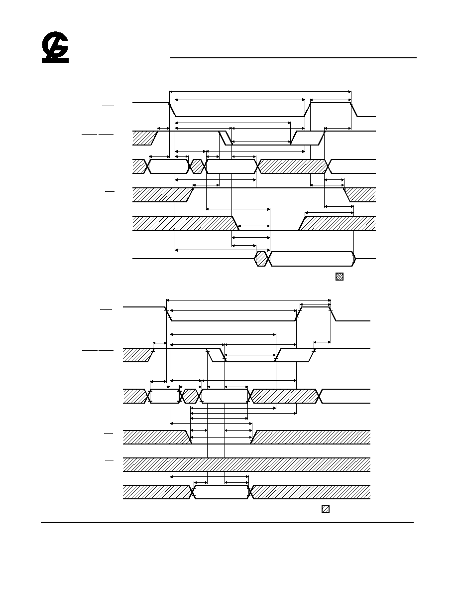
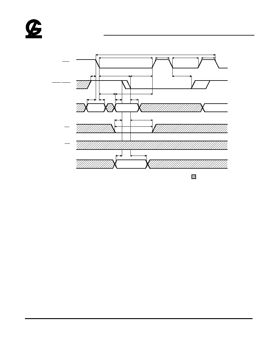
Read CYCLE
Note : D
IN
= OPEN
ROW
ADDRESS
COLUMN
ADDRESS
DATA-OUT
t
RC
t
RAS
t
RP
t
CRP
t
CSH
t
RCD
t
RSH
t
CAS
t
CRP
t
ASR
t
RAH
t
RAD
t
ASC
t
CAH
t
RAL
t
RCH
t
RRH
t
AR
t
RCS
t
AA
t
OEA
t
CEZ
t
OEZ
t
CAC
t
CLZ
t
RAC
Don't Care
V
IH-
V
IL-
RAS
V
IH-
V
IL-
UCAS,LCAS
V
IH-
V
IL-
Address
V
IH-
V
IL-
WE
V
IH-
V
IL-
OE
V
OH-
V
OL-
DQ
Early Write Cycle
NOTE : D
OUT
= OPEN
t
RP
t
RC
t
CRP
t
CSH
t
CRP
t
RCD
t
RSH
t
CAS
t
ASR
t
RAH
t
RAD
t
ASC
t
CAH
t
RAL
t
CWL
t
RWL
t
WCR
t
WCH
t
WP
t
WCS
t
AR
t
DS
t
DH
t
DHR
DATA - IN
COLUMN
ADDRESS
ROW
ADDRESS
V
IH-
V
IL-
RAS
V
IH-
V
IL-
UCAS,LCAS
V
IH-
V
IL-
Address
V
IH-
V
IL-
WE
V
IH-
V
IL-
OE
V
IH-
V
IL-
DQ
Don't Care
t
RAS
G -LINK
GLT4160L16
1M X 16 CMOS DYNAMIC RAM WITH EXTENDED DATA OUTPUT
Apr 2003 (Rev.4.1)
G-Link Technology Corporation,Taiwan
Web : www.glink.com.tw Email : sales@glink.com.tw
TEL : 886-2-26599658
- 9 -
OE Controlled Write Cycle
NOTE : D
OUT
= OPEN
t
RP
t
RC
t
CRP
t
CSH
t
CRP
t
RCD
t
RSH
t
CAS
t
ASR
t
RAH
t
RAD
t
ASC
t
CAH
t
RAL
DATA - IN
COLUMN
ADDRESS
ROW
ADDRESS
V
IH-
V
IL-
RAS
V
IH-
V
IL-
UCAS,LCAS
V
IH-
V
IL-
Address
V
IH-
V
IL-
WE
V
IH-
V
IL-
OE
V
IH-
V
IL-
DQ
Don't Care
t
RAS
t
RCS
t
CWL
t
RWL
t
WP
t
DS
t
OED
t
OEH
t
DH
Read - Modify - Write Cycle
t
RP
t
RC
t
CRP
t
CRP
t
RCD
t
RSH
VALID
DATA-OUT
COLUMN
ADDRESS
ROW
ADDR.
V
IH-
V
IL-
RAS
V
IH-
V
IL-
UCAS,LCAS
V
IH-
V
IL-
Address
V
IH-
V
IL-
WE
V
IH-
V
IL-
OE
V
I/OH-
V
I/OL-
DQ
Don't Care
t
RAS
VALID
DATA-IN
t
CAS
t
ASR
t
RAH
t
RAD
t
ASC
t
CAH
t
CSH
t
AWD
t
CWD
t
RWL
t
CWL
t
WP
t
OEA
t
CLZ
t
CAC
t
AA
t
RAC
t
DH
t
DS
t
OED
t
OEZ
G -LINK
GLT4160L16
1M X 16 CMOS DYNAMIC RAM WITH EXTENDED DATA OUTPUT
Apr 2003 (Rev.4.1)
G-Link Technology Corporation,Taiwan
Web : www.glink.com.tw Email : sales@glink.com.tw
TEL : 886-2-26599658
- 10 -
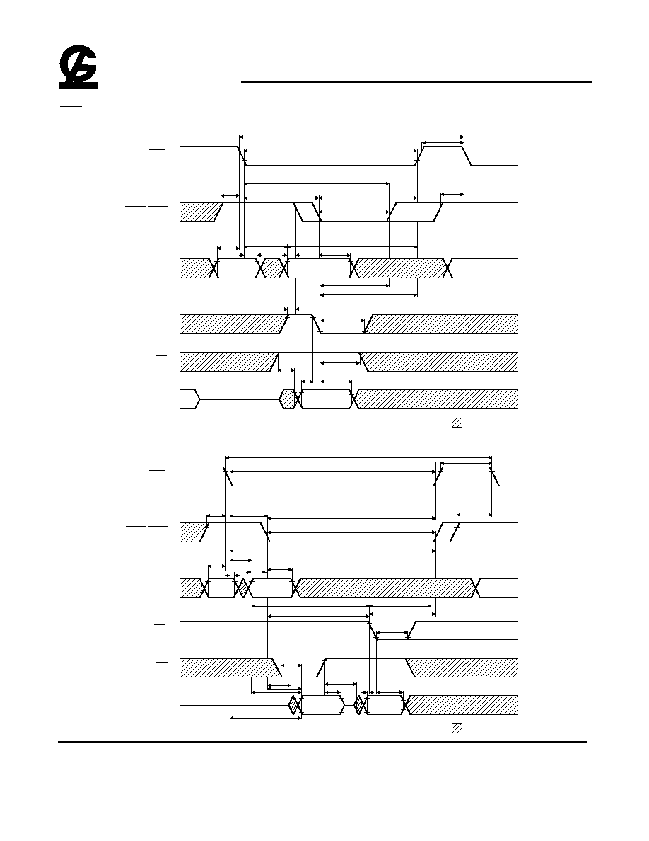
EDO Page Mode Read Cycle
t
RASP
t
RP
t
CRP
t
RCD
t
CAS
t
CSH
t
CP
t
CAS
t
CAS
t
CAS
t
CP
t
CP
t
PC
t
PC
t
PC
t
CSR
t
RAH
t
RAD
t
ASC
t
ASC
t
ASC
t
ASC
t
CAH
t
CAH
t
CAH
t
CAH
t
RCS
t
RCH
t
RRH
t
OEA
t
OEA
t
CAC
t
CPA
t
AA
t
OCH
t
CPA
t
AA
t
CAC
t
OEP
t
CHO
t
AA
t
CAC
t
CPA
t
CLZ
t
OLZ
t
RAC
t
CAC
t
DOH
t
OEZ
t
OEP
t
OEZ
t
OEZ
VALID
DATA-OUT
VALID
DATA-OUT
VALID
DATA-OUT
VALID
DATA-OUT
VALID
DATA-OUT
V
IH-
V
IL-
RAS
V
IH-
V
IL-
UCAS,LCAS
V
IH-
V
IL-
Address
V
IH-
V
IL-
WE
V
IH-
V
IL-
OE
DQ
V
OH-
V
OL-
ROW
ADDR.
COLUMN
ADDRESS
COLUMN
ADDRESS
COL.
ADDR.
COL.
ADDR.
Don't Care
EDO Page Mode Early Write Cycle
NOTE : D
OUT
= OPEN
t
RASP
t
RP
t
CRP
t
RCD
t
CAS
V
IH-
V
IL-
RAS
V
IH-
V
IL-
UCAS,LCAS
t
CAS
t
CAS
t
CP
t
CP
t
PC
t
PC
t
RSH
t
ASR
t
RAD
t
RAH
t
ASC
t
CAH
t
CSH
t
ASC
t
ASC
t
CAH
t
CAH
t
WCS
t
WP
t
WCH
t
WCS
t
WCS
t
WCH
t
WCH
t
WP
t
WP
t
DS
t
DS
t
DS
t
DH
t
DS
t
DS
V
IH-
V
IL-
Address
V
IH-
V
IL-
WE
V
IH-
V
IL-
OE
DQ
V
IH-
V
IL-
ROW
ADDR.
COLUMN
ADDRESS
COLUMN
ADDRESS
COLUMN
ADDRESS
VALID
DATA-IN
VALID
DATA-IN
VALID
DATA-IN
Don't Care

G -LINK
GLT4160L16
1M X 16 CMOS DYNAMIC RAM WITH EXTENDED DATA OUTPUT
Apr 2003 (Rev.4.1)
G-Link Technology Corporation,Taiwan
Web : www.glink.com.tw Email : sales@glink.com.tw
TEL : 886-2-26599658
- 11 -
EDO Page Mode Read - Modify - Write Cycle
t
RASP
t
RP
V
IH-
V
IL-
RAS
V
IH-
V
IL-
UCAS,LCAS
Don't Care
t
CSH
t
RCD
t
CAS
t
CP
t
CAS
t
RSH
t
CRP
t
RAD
t
RAH
t
ASR
t
ASC
t
CAH
t
ASC
t
CAH
t
RAL
t
PRWC
t
RCS
t
WP
t
CWL
t
WP
t
CWL
t
RWL
t
CWD
t
AWD
t
RWD
t
OEA
t
CWD
t
AWD
t
CPWD
t
OEA
t
OEH
t
RAC
t
AA
t
CAC
t
OEZ
t
OED
t
DS
t
DH
t
AA
t
CAC
t
OEZ
t
OED
t
DS
t
DH
t
CLZ
t
CLZ
VALID
DATA-OUT
VALID
DATA-IN
VALID
DATA-OUT
VALID
DATA-IN
ROW
ADDR.
COL.
ADDR.
COL.
ADDR.
V
IH-
V
IL-
Address
V
IH-
V
IL-
WE
V
IH-
V
IL-
OE
V
I/OH-
V
I/OL-
DQ
CAS - Before - RAS Refresh Cycle
V
IH-
V
IL-
RAS
t
RAS
t
RAS
t
RP
t
RP
t
RC
t
RC
t
CSR
t
CSR
t
CHR
t
CHR
t
RPC
t
RPC
t
CRP
V
IH-
V
IL-
UCAS,LCAS
Remark Address, WE, OE : Don't care DQ : Hi-Z
RAS -Only Refresh Cycle
V
IH-
V
IL-
RAS
t
RAS
t
RAS
t
RP
t
RP
t
RC
t
RC
t
RPC
t
CRP
V
IH-
V
IL-
UCAS,LCAS
t
CRP
t
ASR
t
ASR
t
RAH
t
RAH
ROW
ADDRESS
ROW
ADDRESS
Address
V
IH-
V
IL-
Remark WE, OE : Don't care DQ : Hi-Z
G -LINK
GLT4160L16
1M X 16 CMOS DYNAMIC RAM WITH EXTENDED DATA OUTPUT
Apr 2003 (Rev.4.1)
G-Link Technology Corporation,Taiwan
Web : www.glink.com.tw Email : sales@glink.com.tw
TEL : 886-2-26599658
- 12 -
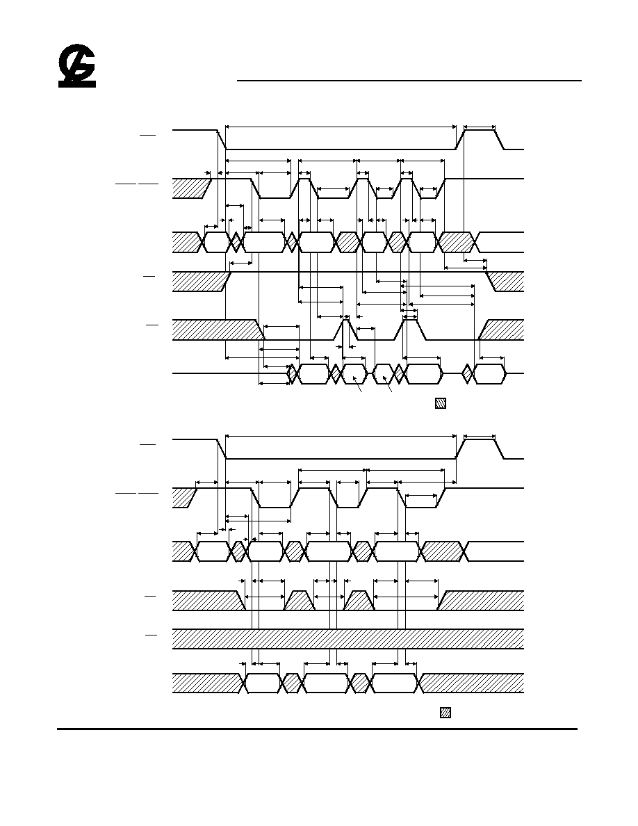
CAS
- Before -
RAS
Self Refresh Cycle
V
IH-
V
IL-
RAS
t
CP
t
RP
t
RASS
t
CP
t
CHS
V
IH-
V
IL-
UCAS
t
CSR
V
IH-
V
IL-
LCAS
t
CHS
t
RPC
t
RPC
t
CP
t
CSR
t
CEZ
OPEN
OPEN
V
IH-
V
IL-
DQ
0
~DQ
7
V
IH-
V
IL-
DQ
8
~DQ
15
Don't Care
NOTE : WE , OE ,Address = Don't care.
Hidden Refresh Cycle ( Read )
t
RP
t
CRP
t
RCD
V
IH-
V
IL-
RAS
V
IH-
V
IL-
UCAS,LCAS
t
RAC
V
IH-
V
IL-
Address
V
IH-
V
IL-
WE
V
IH-
V
IL-
OE
DQ
V
IH-
V
IL-
ROW
ADDRESS
Don't Care
t
RP
t
CAC
t
RCS
t
ASC
t
CAH
t
ASR
t
CAH
t
RAD
t
RAL
t
RSH
t
CHR
t
RC
t
RAS
t
RAS
COLUMN
ADDRESS
t
RC
t
WHR
t
AA
t
OEA
t
CLZ
t
REZ
t
CEZ
t
WEZ
t
OEZ
DATA-OUT
OPEN
G -LINK
GLT4160L16
1M X 16 CMOS DYNAMIC RAM WITH EXTENDED DATA OUTPUT
Apr 2003 (Rev.4.1)
G-Link Technology Corporation,Taiwan
Web : www.glink.com.tw Email : sales@glink.com.tw
TEL : 886-2-26599658
- 13 -
Hidden Refresh Cycle ( Write )
NOTE : D
OUT
= OPEN
t
RP
t
CRP
t
RCD
V
IH-
V
IL-
RAS
V
IH-
V
IL-
UCAS,LCAS
t
DS
V
IH-
V
IL-
Address
V
IH-
V
IL-
WE
V
IH-
V
IL-
OE
DQ
V
IH-
V
IL-
ROW
ADDRESS
Don't Care
t
RP
t
DH
t
WP
t
WCH
t
WCS
t
ASC
t
CAH
t
ASC
t
CAH
t
RAD
t
RSH
t
RSH
t
CHR
t
RC
t
RAS
t
RAS
COLUMN
ADDRESS
DATA-IN

G -LINK
GLT4160L16
1M X 16 CMOS DYNAMIC RAM WITH EXTENDED DATA OUTPUT
Apr 2003 (Rev.4.1)
G-Link Technology Corporation,Taiwan
Web : www.glink.com.tw Email : sales@glink.com.tw
TEL : 886-2-26599658
- 14 -
CAS ≠Before- RAS Refresh Counter Test Cycle
t
CAS
t
CPT
V
IH-
V
IL-
RAS
V
IH-
V
IL-
CAS
t
RP
t
RAS
t
CSR
t
CHR
t
RSH
t
RAL
t
ASC
t
AA
t
CAC
t
RCS
t
RRH
t
RCH
t
OEA
t
CEZ
t
OEZ
t
CLZ
t
RWL
t
CWL
t
WCH
t
WCS
t
WP
t
DS
t
DH
t
RCS
t
AWD
t
CWD
t
RWL
t
CWL
t
WP
t
DH
t
DS
t
OED
t
OEZ
t
CLZ
t
CAC
t
AA
t
OEA
OPEN
COLUMN
ADDRESS
VALID DATA-OUT
VALID DATA-IN
Don't Care
VALID
DATA-IN
VALID
DATA-OUT
V
IH-
V
IL-
Address
V
IH-
V
IL-
WE
V
IH-
V
IL-
OE
V
OH-
V
OL-
DQ
V
IH-
V
IL-
WE
V
IH-
V
IL-
OE
V
IH-
V
IL-
DQ
V
IH-
V
IL-
WE
V
IH-
V
IL-
OE
V
I/OH-
V
I/OL-
DQ
Read Cycle
Write Cycle
Read-Modify-Write
t
CAH
G -LINK
GLT4160L16
1M X 16 CMOS DYNAMIC RAM WITH EXTENDED DATA OUTPUT
Apr 2003 (Rev.4.1)
G-Link Technology Corporation,Taiwan
Web : www.glink.com.tw Email : sales@glink.com.tw
TEL : 886-2-26599658
- 15 -
Ordering Information
Part Number
SPEED
POWER
FEATURE TEMPERATUR
PACKAGE
GLT4160L16-45J4
45ns
Normal
EDO
Commercial
42L 400mil SOJ
GLT4160L16-50J4
50ns
Normal
EDO
Commercial
42L 400mil SOJ
GLT4160L16-60J4
60ns
Normal
EDO
Commercial
42L 400mil SOJ
GLT4160L16-70J4
70ns
Normal
EDO
Commercial
42L 400mil SOJ
GLT4160L16S-45J4
45ns
Self Refresh
EDO
Commercial
42L 400mil SOJ
GLT4160L16S-50J4
50ns
Self Refresh
EDO
Commercial
42L 400mil SOJ
GLT4160L16S-60J4
60ns
Self Refresh
EDO
Commercial
42L 400mil SOJ
GLT4160L16S-70J4
70ns
Self Refresh
EDO
Commercial
42L 400mil SOJ
GLT4160L16P-45J4
45ns
Normal
EDO
Commercial
42L 400mil SOJ
GLT4160L16P-50J4
50ns
Normal
EDO
Commercial
42L 400mil SOJ
GLT4160L16P-60J4
60ns
Normal
EDO
Commercial
42L 400mil SOJ
GLT4160L16P-70J4
70ns
Normal
EDO
Commercial
42L 400mil SOJ
GLT4160L16SP-45J4
45ns
Self Refresh
EDO
Commercial
42L 400mil SOJ
GLT4160L16SP-50J4
50ns
Self Refresh
EDO
Commercial
42L 400mil SOJ
GLT4160L16SP-60J4
60ns
Self Refresh
EDO
Commercial
42L 400mil SOJ
GLT4160L16SP-70J4
70ns
Self Refresh
EDO
Commercial
42L 400mil SOJ
GLT4160L16-45TC
45ns
Normal
EDO
Commercial
44/50L 400mil TSOPII
GLT4160L16-50TC
50ns
Normal
EDO
Commercial
44/50L 400mil TSOPII
GLT4160L16-60TC
60ns
Normal
EDO
Commercial
44/50L 400mil TSOPII
GLT4160L16-70TC
70ns
Normal
EDO
Commercial
44/50L 400mil TSOPII
GLT4160L16S-45TC
45ns
Self Refresh
EDO
Commercial
44/50L 400mil TSOPII
GLT4160L16S-50TC
50ns
Self Refresh
EDO
Commercial
44/50L 400mil TSOPII
GLT4160L16S-60TC
60ns
Self Refresh
EDO
Commercial
44/50L 400mil TSOPII
GLT4160L16S-70TC
70ns
Self Refresh
EDO
Commercial
44/50L 400mil TSOPII
GLT4160L16P-45TC
45ns
Normal
EDO
Commercial
44/50L 400mil TSOPII
GLT4160L16P-50TC
50ns
Normal
EDO
Commercial
44/50L 400mil TSOPII
GLT4160L16P-60TC
60ns
Normal
EDO
Commercial
44/50L 400mil TSOPII
GLT4160L16P-70TC
70ns
Normal
EDO
Commercial
44/50L 400mil TSOPII
GLT4160L16SP-45TC
45ns
Self Refresh
EDO
Commercial
44/50L 400mil TSOPII
GLT4160L16SP-50TC
50ns
Self Refresh
EDO
Commercial
44/50L 400mil TSOPII
GLT4160L16SP-60TC
60ns
Self Refresh
EDO
Commercial
44/50L 400mil TSOPII
GLT4160L16SP-70TC
70ns
Self Refresh
EDO
Commercial
44/50L 400mil TSOPII
GLT4160L16E-45J4
45ns
Normal
EDO
Commercial
42L 400mil SOJ
GLT4160L16E-50J4
50ns
Normal
EDO
Commercial
42L 400mil SOJ
GLT4160L16E-60J4
60ns
Normal
EDO
Commercial
42L 400mil SOJ
GLT4160L16E-70J4
70ns
Normal
EDO
Commercial
42L 400mil SOJ
GLT4160L16EP-45J4
45ns
Normal
EDO
Commercial
42L 400mil SOJ
GLT4160L16EP-50J4
50ns
Normal
EDO
Commercial
42L 400mil SOJ
GLT4160L16EP-60J4
60ns
Normal
EDO
Commercial
42L 400mil SOJ
GLT4160L16EP-70J4
70ns
Normal
EDO
Commercial
42L 400mil SOJ
GLT4160L16SE-45J4
45ns
Self Refresh
EDO
Commercial
42L 400mil SOJ
GLT4160L16SE-50J4
50ns
Self Refresh
EDO
Commercial
42L 400mil SOJ
GLT4160L16SE-60J4
60ns
Self Refresh
EDO
Commercial
42L 400mil SOJ
GLT4160L16SE-70J4
70ns
Self Refresh
EDO
Commercial
42L 400mil SOJ
GLT4160L16SEP-45J4
45ns
Self Refresh
EDO
Commercial
42L 400mil SOJ
GLT4160L16SEP-50J4
50ns
Self Refresh
EDO
Commercial
42L 400mil SOJ
GLT4160L16SEP-60J4
60ns
Self Refresh
EDO
Commercial
42L 400mil SOJ
GLT4160L16SEP-70J4
70ns
Self Refresh
EDO
Commercial
42L 400mil SOJ
GLT4160L16E-45TC
45ns
Normal
EDO
Commercial
44/50L 400mil TSOPII
GLT4160L16E-50TC
50ns
Normal
EDO
Commercial
44/50L 400mil TSOPII
GLT4160L16E-60TC
60ns
Normal
EDO
Commercial
44/50L 400mil TSOPII
GLT4160L16E-70TC
70ns
Normal
EDO
Commercial
44/50L 400mil TSOPII
GLT4160L16SE-45TC
45ns
Self Refresh
EDO
Commercial
44/50L 400mil TSOPII
GLT4160L16SE-50TC
50ns
Self Refresh
EDO
Commercial
44/50L 400mil TSOPII
GLT4160L16SE-60TC
60ns
Self Refresh
EDO
Commercial
44/50L 400mil TSOPII
GLT4160L16SE-70TC
70ns
Self Refresh
EDO
Commercial
44/50L 400mil TSOPII
GLT4160L16SEP-45TC
45ns
Self Refresh
EDO
Commercial
44/50L 400mil TSOPII
GLT4160L16SEP-50TC
50ns
Self Refresh
EDO
Commercial
44/50L 400mil TSOPII
GLT4160L16SEP-60TC
60ns
Self Refresh
EDO
Commercial
44/50L 400mil TSOPII
GLT4160L16SEP-70TC
70ns
Self Refresh
EDO
Commercial
44/50L 400mil TSOPII
G -LINK
GLT4160L16
1M X 16 CMOS DYNAMIC RAM WITH EXTENDED DATA OUTPUT
Apr 2003 (Rev.4.1)
G-Link Technology Corporation,Taiwan
Web : www.glink.com.tw Email : sales@glink.com.tw
TEL : 886-2-26599658
- 16 -
Parts Numbers (Top Mark) Definition :
GLT 4 160 L 16 P - 40 TC
4 : DRAM
5 : Synchronous
DRAM
6 : Standard
SRAM
7 : Cache SRAM
8 : Synchronous
Burst SRAM
9 : SGRAM
-SRAM
064 : 8K
256 : 256K
512 : 512K
100 : 1M
200 : 2M
400 : 4M
-DRAM
10 : 1M(C/EDO)
11 : 1M(C/FPM)
12 : 1M(H/EDO)
13 : 1M(H/FPM)
20 : 2M(EDO)
21 : 2M(FPM)
40 : 4M(EDO)
41 : 4M(FPM)
80 : 8M(EDO)
81 : 8M(FPM)
160 : 16M(EDO)
161 : 16M(FPM)
640 : 64M(EDO)
641 : 64M(FPM)
-SDRAM
40 : 4M
160 : 16M
320 : 32M,4Bank
640 : 64M
128 : 128M
VOLTAGE
Blank : 5V
L : 3.3V
M : 2.5V
N : 2.0V
CONFIG.
04 : x04
08 : x08
16 : x16
32 : x32
SPEED
-SRAM
12 : 12ns
15 : 15ns
20 : 20ns
55 : 55ns
70 : 70ns
85 : 85ns
120 : 120ns
-DRAM
25 : 25ns
28 : 28ns
30 : 30ns
35 : 35ns
40 : 40ns
45 : 45ns
50 : 50ns
60 : 60ns
70 : 70ns
80 : 80ns
100 : 100ns
SDRAM :
5 : 5ns/200 MHZ
5.5 : 5.5ns/183 MHZ
6 : 6ns/166 MHZ
7 : 7ns/143 MHZ
8 : 8ns/125 MHZ
10 : 10ns/100 MHZ
PACKAGE
T : PDIP(300mil)
TS : TSOP(Type I)
ST : sTSOP(Type I)
TC : TSOPll (40/44)
PL : PLCC
FA : 300mil SOP
FB : 330mil SOP
FC : 445mil SOP
J3 : 300mil SOJ
J4 : 400mil SOJ
P : PDIP(600mil)
Q : PQFP
TQ : TQFP
FG : 48Pin BGA 9x12
FH : 48Pin BGA 8x10
FI : 48Pin BGA 6x8
FJ : 60Ball VFBGA
POWER
Blank : Standard
L : Low Power
LL : Low Low Power
SL : Super Low Power
Temperature Range
E : Extended Temperature
I : Industrial Temperature
Blank : Commercial Temperature
P : Pb ≠ free part
G -LINK
GLT4160L16
1M X 16 CMOS DYNAMIC RAM WITH EXTENDED DATA OUTPUT
Apr 2003 (Rev.4.1)
G-Link Technology Corporation,Taiwan
Web : www.glink.com.tw Email : sales@glink.com.tw
TEL : 886-2-26599658
- 17 -
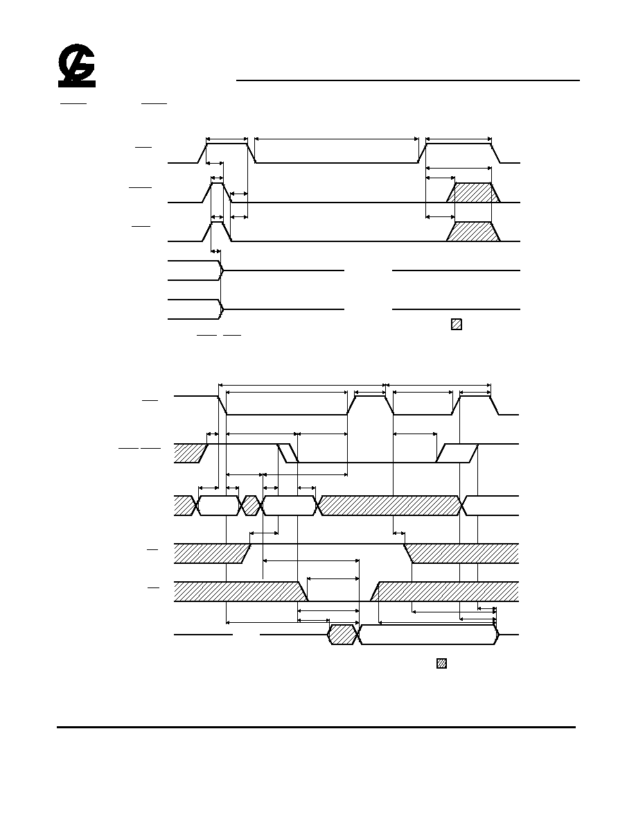
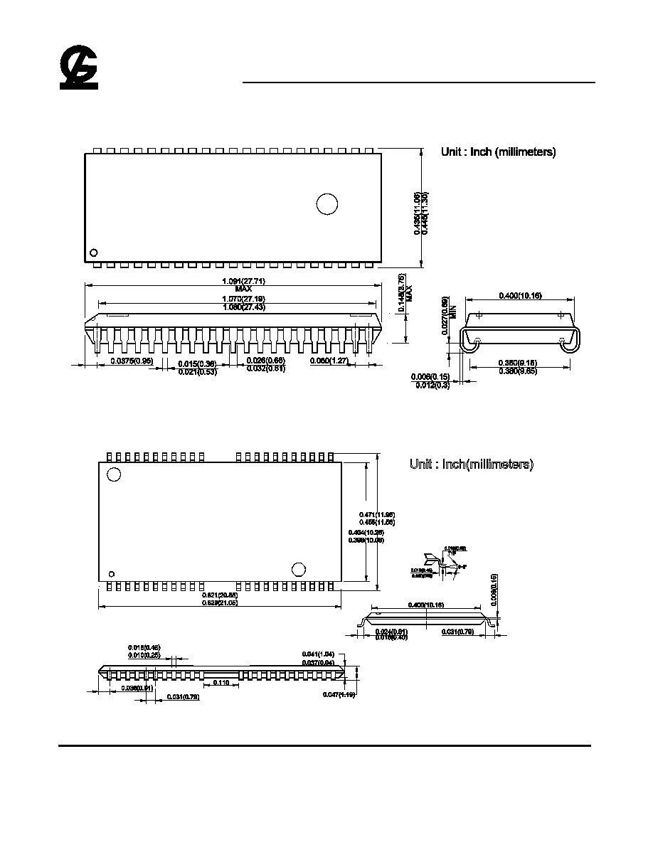
Package Information
40/42L 400MIL SOJ
44/50L TSOPII 400MIL