G -LINK
GLT4160M16
1M X 16 CMOS DYNAMIC RAM WITH EXTENDED DATA OUTPUT
Dec 2001 (Rev.1.1)
G-Link Technology Corporation
2701Northwestern Parkway
Santa Clara, CA 95051, U.S.A.
G-Link Technology Corporation,Taiwan
6F, No. 24-2, Industry E. RD. IV, Science Based
Industrial Park, Hsin Chu, Taiwan.
- 1 -
Features :
Description :
1,048,576
words by 16 bits organization.
Fast access time and cycle time.
Dual
CAS
Input.
Low power dissipation.
Read-Modify-Write,
RAS
-Only Refresh,
CAS
-Before-
RAS
Refresh, Hidden
Refresh and Test Mode Capability.
1024 refresh cycles per 16ms.
Available in 400 mil TSOPII Packages.
Single 2.5V
�
0.2V Power Supply.
All inputs and Outputs are LVTTL
compatible.
Extended Data-Out(EDO) Page Mode
operation.
Self � refresh capability. (S-Version).
Extended Temperature Available
( -25
�
C ~ 85
�
C )
The GLT4160M16 is a 1,048,576 x 16
bit high-performance CMOS dynamic random
access memory. The GLT4160M16 offers
Fast Page mode with Extended Data Output,
and has both BYTE WRITE and WORD
WRITE access cycles via two
CAS
pins. The
GLT4160M16 has symmetric address and
accepts 1024-cycle refresh in 16ms interval.
All inputs are TTL compatible. EDO
Page Mode operation allows random access
up to 1024 x 16 bits within a page, with cycle
times as short as 25ns.
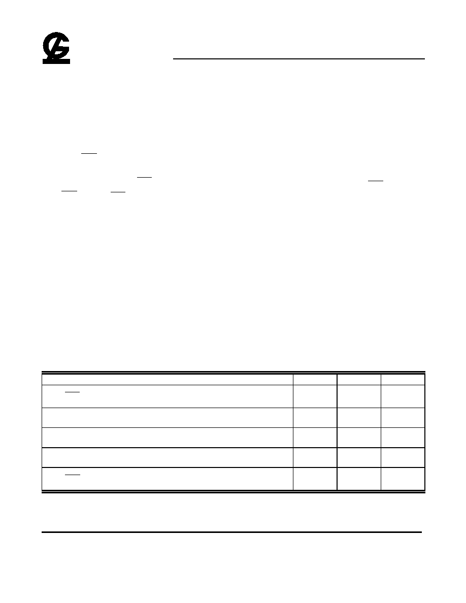
HIGH PERFORMANCE
60
70
80
Max.
RAS
Access Time, (t
RAC
)
60 ns
70 ns
80 ns
Max. Column Address Access Time, (t
CAA
)
30 ns
35 ns
40 ns
Min. Extended Data Out Page Mode Cycle Time, (t
PC
)
25 ns
30 ns
35 ns
Min. Read/Write Cycle Time, (t
RC
)
104 ns
124 ns
144 ns
Max.
CAS
Access Time (t
CAC
)
15 ns
20 ns
20 ns

G -LINK
GLT4160M16
1M X 16 CMOS DYNAMIC RAM WITH EXTENDED DATA OUTPUT
Dec 2001 (Rev.1.1)
G-Link Technology Corporation
2701Northwestern Parkway
Santa Clara, CA 95051, U.S.A.
G-Link Technology Corporation,Taiwan
6F, No. 24-2, Industry E. RD. IV, Science Based
Industrial Park, Hsin Chu, Taiwan.
- 2 -
Pin Configuration :
Vcc
DQ
0
A0
A1
1
2
3
4
5
6
7
9
10
12
13
14
NC
OE
LCAS
V
SS
DQ
15
DQ
1
WE
RAS
NC
A
9
A
8
8
15
16
17
18
19
20
21
24
25
26
27
28
29
30
31
32
33
35
36
37
38
39
40
41
42
43
44
DQ
2
DQ
3
Vcc
DQ
4
DQ
5
DQ
6
DQ
7
NC
A2
DQ
14
DQ
13
DQ
12
V
SS
DQ
11
DQ
10
DQ
9
DQ
8
UCAS
A
7
A
6
A
5
TSOP(Type II)
Top View
V
CC
22
23
V
SS
34
11
NC
NC
NC
A3
NC
A
4
Pin Descriptions:
Name
Function
A
0
- A
9
Address Inputs
RAS
Row Address Strobe
UCAS
Column Address Strobe/Upper Byte Control
LCAS
Column Address Strobe/Lower Byte Control
WE
Write Enable
OE
Output Enable
DQ
0
- DQ
15
Data Inputs / Outputs
V
CC
+2.5V Power Supply
V
SS
Ground
NC
No Connection
G -LINK
GLT4160M16
1M X 16 CMOS DYNAMIC RAM WITH EXTENDED DATA OUTPUT
Dec 2001 (Rev.1.1)
G-Link Technology Corporation
2701Northwestern Parkway
Santa Clara, CA 95051, U.S.A.
G-Link Technology Corporation,Taiwan
6F, No. 24-2, Industry E. RD. IV, Science Based
Industrial Park, Hsin Chu, Taiwan.
- 3 -
Absolute Maximum Ratings*
Capacitance*
T
A
=25
�
C, V
CC
=2.5V
�
0.2V, V
SS
=0V
Symbol
Parameter
Max.
Unit
C
IN1
Address Input
5
pF
C
IN2
RAS
,
LCAS
,
UCAS
,
WE
,
OE
7
pF
Operating Temperature, T
A
(ambient)
........................................0
�
C to +70
�
C
.............................(extended)..�25
�
C to +85
�
C
Storage Temperature(plastic).....-55
�
C to +150
�
C
Voltage Relative to V
SS
................-1.0V to + 3.5V
Short Circuit Output Current.......................50mA
Power Dissipation........................................1.0W
C
OUT
Data Input/Output
7
pF
*Note:Operation above Absolute Maximum Ratings can
abversely affect device reliability.
*Note: Capacitance is sampled and not 100% tested
Electrical Specifications
l
CAS
means
UCAS
and
LCAS
.
l
All voltages are referenced to GND.
l
After power up, wait more than 200
�
s and then, execute eight
CAS
-before-
RAS
or
RAS
-only
refresh cycles as dummy cycles to initialize internal circuit.
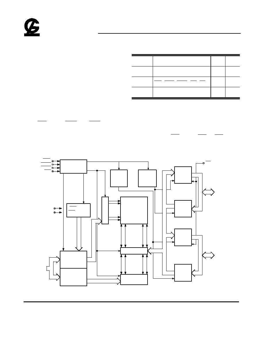
Block Diagram :
Memory
Array
1024X1024X16
Upper
Byte
Control
Sense Amplifier
Column Decoder
Row
Address
Buffer
Column
Address
Buffer
...1024X16...
...1024...
....1024....
Lower
Byte
Control
Row Decoder
Data
Output
Buffer
Data
Input
Buffer
Data
Output
Buffer
Data
Input
Buffer
CAS before
RAS Counter
Clock
Generator
A0
|
A9
X0..X9
Y0..Y9
DQ8
|
DQ15
DQ0
|
DQ7
RAS
LCAS
UCAS
WE
Vcc
GND
OE
X8
X8
X8
X8
X8
X1
6
X8
X8
X8

G -LINK
GLT4160M16
1M X 16 CMOS DYNAMIC RAM WITH EXTENDED DATA OUTPUT
Dec 2001 (Rev.1.1)
G-Link Technology Corporation
2701Northwestern Parkway
Santa Clara, CA 95051, U.S.A.
G-Link Technology Corporation,Taiwan
6F, No. 24-2, Industry E. RD. IV, Science Based
Industrial Park, Hsin Chu, Taiwan.
- 4 -
DC and Operating Characteristics (1-2)
T
A
= 0
�
C to 70
�
C, -25
�
C to 85
�
C (extended temperature) V
CC
=2.5V
�
0.2V, V
SS
=0V, unless otherwise specified.
Sym.
Parameter
Test Conditions
Access
Time
Min. Typ Max. Unit Notes
I
LI
Input Leakage Current
(any input pin)
0V
V
IN
Vcc+0.3V
(All other pins not under test=0V)
-5
+5
�
A
I
LO
Output Leakage Current
(for High-Z State)
0V
V
out
Vcc
Output is disabled (Hiz)
-5
+5
�
A
I
CC1
Operating Current,
Random READ/WRITE
t
RC
= t
RC
(min.)
t
RAC
= 60ns
t
RAC
= 70ns
t
RAC
= 80ns
140
130
120
mA
1,2
I
CC2
Standby Current,(TTL)
RAS , UCAS , LCAS at V
IH
other inputs
V
SS
1
mA
I
CC3
Refresh Current,
RAS -Only
RAS cycling, UCAS , LCAS at V
IH
t
RC
= t
RC
(min.)
t
RAC
= 60ns
t
RAC
= 70ns
t
RAC
= 80ns
140
130
120
mA
2
I
CC4
Operating Current,
EDO Page Mode
RAS at V
IL
, UCAS , LCAS address
cycling:t
PC
=t
PC
(min.)
t
RAC
= 60ns
t
RAC
= 70ns
t
RAC
= 80ns
140
130
120
mA
1,2
I
CC5
Refresh Current,
CAS Before RAS
RAS , UCAS , LCAS
address cycling:
t
RC
=t
RC
(min.)
t
RAC
= 60ns
t
RAC
= 70ns
t
RAC
= 80ns
140
130
120
mA
1
I
CC6
Standby Current,
(CMOS)
RAS
V
CC
-0.2V,
UCAS
V
CC
-0.2V,
LCAS
V
CC
-0.2V,
All other inputs V
SS
200
�
A
1,5
I
CC7
Self Refresh Current
RAS = UCAS = LCAS =V
IL
WE = OE =A
0
~A
9
=V
CC
-0.2V or 0.2V
DQ
0
~DQ
15
=V
CC
-0.2V,0.2V or Open
200
�
A
V
IL
Input Low Voltage
-0.3
+0.8
V
3
V
IH
Input High Voltage
2.0
V
CC
+0.3
V
3
V
OL
Output Low Voltage
I
OL
= 2mA
0.4
V
V
OH
Output High Voltage
I
OH
= -2mA
2
V
Notes:
1.I
CC
is dependent on output loading when the device output is selected. Specified I
CC
(max.) is measured with the output open.
2.I
CC
is dependent upon the number of address transitions specified I
CC
(max.) is measured with a maximum of one transition per address cycle in
random Read/Write and EDO Fast Page Mode.
3.Specified V
IL
(min.) is steady state operation. During transitions V
IL
(min.) may undershoot to -1.0V for a period not to exceed 15ns. All AC
parameters are measured with V
IL
(min.)
V
SS
and V
IH
(max.)
V
CC
.
4.Specified V
IH
(max.) is steady state operation. During transitions V
IH
(max.) may undershoot to +1.0V for a period not to exceed 15ns. All AC
parameters are measured with V
IL
(min.)
V
SS
and V
IH
(max.)
V
CC
.
5.S-Version.

G -LINK
GLT4160M16
1M X 16 CMOS DYNAMIC RAM WITH EXTENDED DATA OUTPUT
Dec 2001 (Rev.1.1)
G-Link Technology Corporation
2701Northwestern Parkway
Santa Clara, CA 95051, U.S.A.
G-Link Technology Corporation,Taiwan
6F, No. 24-2, Industry E. RD. IV, Science Based
Industrial Park, Hsin Chu, Taiwan.
- 5 -
AC Characteristics
T
A
= 0
�
C to 70
�
C, -25
�
C to 85
�
C (extended temperature),V
CC
= 2.5V
�
0.2V, V
IH
/ V
IL
= 2.0/0 V, V
OH
/V
OL
= 2.0/0.8V
An initial pause of 100
�
s and 8
CAS
-before-
RAS
or
RAS
-only refresh cycles are required after power-up.
60
70
80
Parameter
Symbol
Min.
Max.
Min.
Max.
Min.
Max.
Unit Notes
Read or Write Cycle Time
t
RC
104
124
144
ns
Read Modify Write Cycle Time
t
RWC
140
170
190
ns
RAS
Precharge Time
t
RP
40
50
60
ns
RAS
Pulse Width
t
RAS
60
10k
70
10k
80
10k
ns
Access Time from
RAS
t
RAC
60
70
80
ns
1,2,3
Access Time from
CAS
t
CAC
15
20
20
ns 1,5,10
Access Time from Column Address
t
AA
30
35
40
ns
1,5,6
CAS
to Output Low-Z
t
CLZ
3
3
3
ns
CAS
to Output High-Z
t
CEZ
3
15
3
20
3
20
ns
RAS
Hold Time
t
RSH
15
20
20
ns
RAS
Hold Time Referenced to
OE
t
ROH
10
10
ns
CAS
Hold Time
t
CSH
45
50
70
ns
CAS
Pulse Width
t
CAS
10
10k
15
10k
20
80k
ns
RAS
to CAS Delay Time
t
RCD
20
45
20
50
20
60
ns
RAS
to Column Address Delay Time
t
RAD
15
30
15
35
15
40
ns
7
CAS
to RAS Precharge Time
t
CRP
5
5
5
ns
Row Address Set-Up Time
t
ASR
0
0
0
ns
Row Address Hold Time
t
RAH
10
10
10
ns
Column Address Set-Up Time
t
ASC
0
0
0
ns
Column Address Hold Time
t
CAH
10
15
15
ns
Column Address to RAS Lead Time
t
RAL
30
35
40
ns
Column Address Hold Time Referenced to
RAS
t
AR
45
50
60
ns
Read Command Set-Up Time
t
RCS
0
0
0
ns
Read Command Hold Time Referenced to
CAS
t
RCH
0
0
0
ns
4
Read Command Hold Time Referenced to
RAS
t
RRH
0
0
0
ns
4
Write Command Set-Up Time
t
WCS
0
0
0
ns
8,9
Write Command Hold Time
t
WCH
10
15
15
ns
Write Command Pulse Width
t
WP
10
15
15
ns
Write Command to
RAS
Lead Time
t
RWL
15
30
20
ns
Write Command to
CAS
Lead Time
t
CWL
13
15
20
ns