1
GLT44032-E
128K x 32 Embedded EDO DRAM Macro
F
EATURES
x
Logical organization: 128Kx32 bits
x
Physical organization: 512x256x32
x
Single 3.3v
±
0.3v power supply
x
512-cycle refresh in 8 ms
x
Refresh modes: RAS only, CBR, and Hidden
x
Single CAS with 4 DQM for Byte Write control
x
Non-multiplex row and column addresses
x
Separate I/O operation
x
80/100 MHz page mode EDO cycle
G
ENERAL
D
ESCRIPTION
The GLT44032-E 4Mbit Embedded DRAM (EmDRAM) is
an asynchronous design with non-multiplexed row and
column addressing scheme. RAS, CAS, WE and OE
control the memory operations.
Byte Write operation is controlled by DQM[0], DQM[1],
DQM[2], and DQM[3]. DQM[0] going LOW will mask
DI[0:7] from writing into memory; DQM[1] going LOW
will mask DI[8:15] from writing into memory; DQM[2]
going LOW will mask DI[16:23] from writing into mem-
ory; DQM[3] going LOW will mask DI[24:31] from writing
into memory. All output drivers, DO[0:31], will be Three-
stated during a Write operation.
Performance Data
Parameter
-30
-35
Max. RAS access time, t
RAC
30 ns
35 ns
Max. RAS precharge time, t
RP
20 ns
25 ns
Max. column address access time, t
AA
12 ns
14 ns
Max. CAS access time, t
CAC
8 ns
10 ns
Min. extended data out page mode cycle time, t
PC
10 ns
12.5 ns
Min. read/write cycle time, t
RC
60 ns
70 ns
May 1997 (Rev. 1)

2
G-LINK Technology
GLT44032-E
May 1997 (Rev. 1)
F
UNCTIONAL
B
LOCK
D
IAGRAM
1. V
CC
and V
SS
for the EmDRAM should be separated from the Logic portion of the chip.
Figure 1. GLT44032-E - 128K x 32
CAS
CAS Clock
Generator
CA[7:0]
Memory Array
512 x 256 x 32
WE Clock
Generator
OE
Row Decoders
Data RW
Control
Data I/O
Column Decoders
512
Column
Address
Buffers
WE
Refresh
Counter &
Controller
Row
Address
Buffers
RA[8:0]
RAS Clock
Generator
RAS
Sense Amplifiers
256 x 32
OE Clock
Generator
DO[31:0]
DI[31:0]
AY[7:0]
AX[8:0]
Pin Descriptions
Symbol
Type
Description
DI[31:0]
Input
Data input.
DO[31:0]
Output
Data output.
RA[8:0]
Input
Row address.
CA[7:0]
Input
Column address.
RAS
Input
Row address strobe.
CAS
Input
Column address strobe.
WE
Input
Write enable.
OE Input
Output
enable.
DQM[3:0]
I/O
Data-in mask (active low)
V
CC
[1]
Supply
3.3v voltage supply, 4 pairs double bond minimum
V
SS
[1]
Supply
Ground (voltage return), 4 pairs double bond minimum

3
G-LINK Technology
GLT44032-E
May 1997 (Rev. 1)
Truth Table
Function
RAS
CAS
WE
OE
Address
DQM0
DQM1
DQM2
DQM3
DI[31:0]
DO[31:0]
Standby
H
H
X
X
X
X
X
X
X
X
High-Z
Read
L
L
H
L
Row/Col
X
X
X
X
X
Data Out
Write (Early)
L
L
L
X
Row/Col
H
H
H
H
Data In
High-Z
Write DI[7:0]
L
L
L
X
Row/Col
L
H
H
H
Data In
High-Z
Write DI [15:8]
L
L
L
X
Row/Col
H
L
H
H
Data In
High-Z
Write DI [23:16]
L
L
L
X
Row/Col
H
H
L
H
Data In
High-Z
Write DI [31:24]
L
L
L
X
Row/Col
H
H
H
L
Data In
High-Z
Read-Write
L
L
H
L
L
H
Row/Col
H
H
H
H
Data In
Data Out
Page-Mode Read (First Cycle)
L
H
L
H
L
Row/Col
X
X
X
X
X
Data Out
Page-Mode Read (Subsequent Cycles)
H
L
H
L
Col
X
X
X
X
X
Data Out
Page-Mode Write (First Cycle)
L
H
L
L
X
Row/Col
H
H
H
H
Data In
High-Z
Page-Mode Write (Subsequent Cycle)
L
H
L
L
X
Col
H
H
H
H
Data In
High-Z
Page-Mode R-W (First Cycle)
L
H
L
H
L
L
H
Row/Col
H
H
H
H
Data In
Data Out
Page-Mode R-W (Subsequent Cycle)
L
H
L
H
L
L
H
Col
H
H
H
H
Data In
Data Out
CBR Refresh
H
L
L
X
X
X
X
X
X
X
X
High-Z
RAS-only Refresh
L
H
X
X
Row
X
X
X
X
X
High-Z
4
G-LINK Technology
GLT44032-E
May 1997 (Rev. 1)
E
LECTRICAL
S
PECIFICATIONS
1. Operation above Absolute Maximum ratings can adversely affect device reliability.
1. Capacitance is sampled and not 100% tested
Absolute Maximum Ratings
[1]
Parameter
Rating
Ambient Operating Temperature
0
∞
C to +70
∞
C
Storage Temperature
-50
∞
C to +125
∞
C
Voltage Relative to V
SS
-0.5 V to 4.5 V
Power Dissipation
0.8W
Recommended Operating Conditions
Symbol
Parameter
Min
Typ
Max
Unit
V
CC
Power Supply
3.0
3.3
3.6
V
V
IH
Input High Voltage
2
≠
V
CC
+ 0.3
V
V
IL
Input Low Voltage
-0.5
≠
≠
V
Capacitance
Symbol
Description
Min
Max
Units
Notes
C
IN
Input Capacitance
≠
2
pF
[1]
C
IO
Input/Output Capacitance
≠
2
pF
[1]
DC Characteristics (V
CC
= 3.3V
±
10%, T
A
= 0
∞
C to +70
∞
C)
Symbol
Description
Conditions
-30
-35
Units
Min
Max
Min
Max
V
IH
Input High (Logic 1) Voltage
2.4
V
CC
+1
2.4
V
CC
+1
V
V
IL
Input Low (Logic 0) Voltage
-0.5
0.8
-0.5
0.8
V
V
OH
Output High Voltage
I
OH
= -2.0 mA
2.4
V
CC
2.4
V
CC
V
V
OL
Output Low Voltage
I
OL
= 2 mA
0
0.4
0
0.4
V
I
CC1
Average Power Supply Current (Operating)
RAS, CAS cycling; t
RC
= Min.
≠
200
≠
180
mA
I
CC2
Power Supply Current (Standby)
RAS, CAS = V
IH
≠
1
≠
1
mA
I
CC3
Average Power Supply Current
(RAS-only Refresh)
RAS = cycling; CAS = V
IH
; t
RC
= Min.
≠
200
≠
180
mA
I
CC4
Average Power Supply Current
(Fast Page Mode)
RAS = V
IL
; CAS cycling; t
PC
= Min.
≠
120
≠
100
mA
I
CC4
Average Power Supply Current
(CAS-before-RAS Refresh)
RAS = cycling; CAS before RAS
≠
200
≠
180
mA
5
G-LINK Technology
GLT44032-E
May 1997 (Rev. 1)
1. For better performance margin, switch column addresses and data-in on the rising edge of CAS. Switch DQM on the falling edge of CAS.
2. Set-up time for DQM to CAS going active (low) is 0 ns; hold-time for DQM from CAS going non-active (high) is 4 ns. DQM going low will mask the write.
AC Characteristics (V
CC
= 3.3 V
±
0.3 V, T
A
= 0
∞
C to +70
∞
C, C
L
< 1 pF)
Symbol
Description
-30
-35
Units
Notes
Min
Max
Min
Max
t
RC
Random Read/Write cycle time
60
≠
70
≠
ns
t
PC
Page Mode Read/Write cycle
10
≠
12.5
≠
ns
t
OFF
Read Data valid from RAS high
0
≠
0
≠
ns
t
DOH
Read Data valid from next CAS low
3
≠
3
≠
ns
t
AA
Access time from Column Address
≠
12
≠
14
ns
[1]
t
RAC
Access time from RAS low
≠
30
≠
35
ns
t
CAC
Access time from CAS low
≠
8
≠
10
ns
[1]
t
CPA
Access time from CAS precharge
≠
14
≠
17
ns
[1]
t
RAS
RAS pulse width
30
≠
35
≠
ns
t
RCD
RAS to CAS delay time
15
30
18
35
ns
t
CAS
CAS pulse width
4
≠
5
≠
ns
t
ASR
Row Address setup time
2
≠
2
≠
ns
t
RAH
Row Address hold time
3
≠
4
≠
ns
t
ASC
Column Address setup time
2
≠
2
≠
ns
t
CAH
Column Address hold time
3
≠
4
≠
ns
t
CP
CAS precharge time
4
≠
5
≠
ns
t
CSH
CAS hold time from RAS
30
≠
35
≠
ns
t
DS
Write Data setup time
2
≠
2
≠
ns
t
DH
Write Data hold time
3
≠
4
≠
ns
t
RP
RAS precharge time
20
≠
25
≠
ns
t
CRP
CAS to RAS precharge time
5
≠
10
≠
ns
t
RSH
CAS low to RAS high hold time
5
≠
10
≠
ns
t
RCS
Read command setup time
3
≠
5
≠
ns
t
RCH
Read command hold time from CAS high
3
≠
5
≠
ns
t
RRH
Read command hold time from RAS high
3
≠
5
≠
ns
t
WCS
Write command setup time
3
≠
5
≠
ns
t
WCH
Write command hold time
3
≠
5
≠
ns
t
WP
WE pulse width
8
≠
10
≠
ns
t
T
Transition time (rise and fall)
≠
1.0
≠
1.0
ns
t
RWL
Write command to RAS high
8
≠
10
≠
ns
t
CWL
Write command to CAS high
8
≠
10
≠
ns
t
DMS
DQM mask write setup time to CAS
0
≠
0
≠
ns
[2]
t
DMH
DQM mask write hold time from CAS
3
≠
4
≠
ns
[2]
t
ODW
WE control output disable
8
≠
10
≠
ns
6
G-LINK Technology
GLT44032-E
May 1997 (Rev. 1)
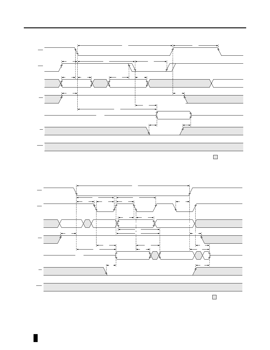
Figure 2. Read Cycle
RAS
CAS
ADDR
DOUT
Don't Care
t
CRP
Row
Column
Row
WE
Valid Data
OE
DQM
t
RCD
t
RAS
t
RP
t
CAS
t
ASR
t
RAH
t
ASC
t
CAH
t
WRP
t
RCH
Hi-Z
t
RAC
t
CAC
t
OE
t
OD
Figure 3. Page Mode Read Cycle
RAS
CAS
ADDR
DOUT
Don't Care
Row
WE
Valid Data
OE
DQM
t
RASP
t
RCD
Hi-Z
Column
Column
t
CAS
t
CP
t
CSH
t
PC
t
RSH
t
ASC
t
CAH
t
WRP
t
RAC
t
CAC
t
OFF
t
OFF
t
RCH
(note 1)
(note 2)
t
OD
Column
t
DOH
t
CAC
t
CPA
t
AA
t
OE

7
G-LINK Technology
GLT44032-E
May 1997 (Rev. 1)
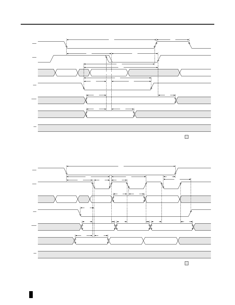
Figure 4. Read/Write Cycle
RAS
CAS
ADDR
DOUT
Don't Care
t
CRP
Row
Column
Row
WE
OE
DQM
t
RCD
t
RAS
t
RP
t
CAS
t
ASR
t
RAH
t
ASC
t
CAH
t
WRP
t
DS
Hi-Z
t
RAC
t
CAC
t
OE
t
OD
DIN
t
DMS
DIN
DOUT
t
WP
t
CWL
t
RWL
t
ODW
t
DH
t
DMH
Figure 5. Page Mode Read/Write Cycle
RAS
CAS
ADDR
DOUT
Don't Care
WE
OE
DQM
t
RASP
t
WRP
t
DS
Hi-Z
t
OE
t
OD
DIN
t
DMS
DIN
t
DH
t
DMH
t
ASR
t
RAH
t
ASC
Row
t
CAH
Column
t
ASC
Column
t
CAH
t
PC
t
CAS
t
CP
t
RWL
t
CWL
t
WP
t
RAC
t
CAC
Column
t
CWL
t
CAC
t
ODW
t
ODW
t
CPA
t
AA
DOUT
DOUT
t
DS
DIN
t
DH
t
DMH
t
DMS
8
G-LINK Technology
GLT44032-E
May 1997 (Rev. 1)
Figure 6. Early Write Cycle
RAS
CAS
ADDR
Don't Care
WE
OE
DQM
t
RAS
DIN
Row
t
RCD
t
RP
t
CAS
Column
t
WCS
t
WCH
t
WP
t
RWL
t
CWL
t
DMS
t
DMH
t
DS
t
DH
Valid Data
Figure 7. Page Mode Early Write Cycle
RAS
CAS
ADDR
Don't Care
WE
OE
DQM
t
RASP
DIN
Row
Column
t
RCD
t
WCH
Column
Column
t
CAS
t
CP
t
CSH
t
CP
t
ASC
t
CAH
t
WCS
t
DMS
t
DS
Valid Data
Valid Data
Valid Data
t
DH
t
DHS
t
DMS
t
DHS
t
DMS
t
RSH
t
DMH

9
G-LINK Technology
GLT44032-E
May 1997 (Rev. 1)

10
G-LINK Technology
GLT44032-E
May 1997 (Rev. 1)

11
G-LINK Technology
GLT44032-E
May 1997 (Rev. 1)

© 2001 G-LINK Technology
All rights reserved. No part of this document may be copied or reproduced in any form or by any means or transferred to any third party without the prior written consent of
G-LINK Technology.
Circuit diagrams utilizing G-LINK products are included as a means of illustrating typical semiconductor applications. Complete information sufficient for design purposes is
not necessarily given.
G-LINK Technology reserves the right to change products or specifications without notice.
The information contained in this document does not convey any license under copyrights, patent rights or trademarks claimed and owned by G-LINK or its subsidiaries.
G-LINK assumes no liability for G-LINK applications assistance, customer's product design, or infringement of patents arising from use of semiconductor devices in such
systems' designs. Nor does G-LINK warrant or represent that any patent right, copyright, or other intellectual property right of G-LINK covering or relating to any combination,
machine, or process in which such semiconductor devices might be or are used.
G-LINK Technology's products are not authorized for use in life support devices or systems. Life support devices or systems are device or systems which are: a) intended for
surgical implant into the human body and b) designed to support or sustain life; and when properly used according to label instructions, can reasonably be expected to cause
significant injury to the user in the event of failure.
The information contained in this document is believed to be entirely accurate. However, G-LINK Technology assumes no responsibility for inaccuracies.
GLT44032-E
www.glinktech.com
G-LINK Technology
1753 South Main Street
Milpitas, California, 95035, USA
TEL: 408-240-1380 ∑ FAX: 408-240-1385
G-LINK Technology Corporation, Taiwan
6F, No. 24-2, Industry E. Rd. IV
Science-Based Industrial Park
Hsin Chu, Taiwan, R.O.C.
TEL: 03-578-2833 ∑ FAX: 03-578-5820
Printed in USA