
1
GLT5160L16
ADVANCED
16M (2-Bank x 524288-Word x 16-Bit) Synchronous DRAM
F
EATURES
u Single 3.3 V ±0.3 V power supply
u Clock frequency 100 MHz / 125 MHz / 143 MHz/
166 MHz
u Fully synchronous operation referenced to clock rising edge
u Dual bank operation controlled by BA (Bank Address)
u CAS latency- 2 / 3 (programmable)
u Burst length- 1 / 2 / 4 / 8 & Full Page (programmable)
u Burst type- sequential / interleave (programmable)
u Industrial grade available
u Byte control by DQMU and DQML
u Column access - random
u Auto precharge / All bank precharge controlled by A[10]
u Auto refresh and Self refresh
u 4096 refresh cycles / 64 ms
u LVTTL Interface
u 400-mil, 50-Pin Thin Small Outline Package (TSOP II) with
0.8 mm lead pitch
u 60-Ball, 6.4mmx10.1mm VFBGA package with 0.65mm Ball
pitch & 0.35mm Ball diameter.
G
ENERAL
D
ESCRIPTION
The GLT5160L16 is a 2-bank x 524288-word x 16-bit Syn-
chronous DRAM, with LVTTL interface. All inputs and
outputs are referenced to the rising edge of CLK. The
GLT5160L16 achieves very high speed data rate up to 166
MHz, and is suitable for main memory or graphic memory in
computer systems.
May. 2003 (Rev.2.4)
∑
∑
∑

2
G-LINK Technology
May. 2003 (Rev. 2.4)
F
UNCTIONAL
B
LOCK
D
IAGRAM
A[10:0]
DQ[15:0]
Figure 1. 16M (2-Bank x 524288-Word x 16-Bit) Synchronous DRAM
C
o
n
t
r
o
l
C
i
r
c
u
i
t
r
y
Address Buffer
BA
CLK
CKE
CS
RAS
Clock Buffer
Control
Signal Buffer
CAS
WE
DQML
DQMU
Mode
Register
Memory Array
Bank #0
Memory Array
Bank #1
I/O Buffer
Signal Description
Signal
Type
Description
CLK
Input
Master Clock: All other inputs are referenced to the rising edge of CLK.
CKE
Input
Clock Enable: CKE controls internal clock. When CKE is low, internal clock for the following cycle is ceased.
CKE is also used to select auto / self refresh. After self refresh mode is started, CKE becomes asynchronous
input. Self refresh is maintained as long as CKE is low.
CS
Input
Chip Select: When CS is high, any command means No Operation.
RAS, CAS, WE
Input
Combination of RAS, CAS, WE defines basic commands.
A[10:0]
Input
A[10:0] specify the Row / Column Address in conjunction with BA. The Row Address is specified by A[10:0].
The Column Address is specified by A[7:0]. A[10] is also used to indicate precharge option. When A[10] is
high at a read / write command, an auto precharge is performed. When A[10] is high at a precharge command,
both banks are precharged.
BA
Input
Bank Address: BA is not simply A[11]. BA specifies the bank to which a command is applied. BA must be set
with ACT, PRE, READ, WRITE commands.
DQ[15:0]
Input / Output
Data In and Data out are referenced to the rising edge of CLK.
DQML
Input
Lower Din[7:0] Mask / Lower Output[7:0] Disable: When DQML is high in burst write, lower Din[7:0] for the
current cycle is masked. When DQML is high in burst read, lower Dout[7:0] is disabled at the next but one
cycle.
DQMU
Input
Upper Din[15:8] Mask / Upper Output[15:8] Disable: When DQMU is high in burst write, upper Din(8-15) for
the current cycle is masked. When DQMU is high in burst read, upper Dout[15:8] is disabled at the next but
one cycle.
V
DD
, V
SS
Power Supply
Power Supply for the memory array and peripheral circuitry.
V
DDQ
, V
SSQ
Power Supply
V
DDQ
and V
SSQ
are supplied to the Output Buffers only.

3
G-LINK Technology
May. 2003 (Rev.2.4)
F
UNCTIONAL
D
ESCRIPTION
The GLT5160L16 provides basic functions, bank (row) activate,
burst read / write, bank (row) precharge, and auto / self refresh.
Each command is defined by control signals of RAS, CAS and WE
at CLK rising edge. In addition to 3 signals, CS, CKE and A[10] are
used as chip select, refresh option, and precharge option,
respectively.
To know the detailed definition of commands, please see the com-
mand truth table.
Activate (ACT) [RAS = L, CAS = WE = H]
ACT command activates a row in an idle bank indicated by BA.
Read (READ) [RAS = H, CAS = L, WE = H]
READ command starts burst read from the active bank indicated by
BA. First output data appears after CAS latency. When A[10] = H at
this command, the bank is deactivated after the burst read (auto-pre-
charge, READA).
Write (WRITE) [RAS = H, CAS =WE = L]
WRITE command starts burst write to the active bank indicated by
BA. Total data length to be written is set by burst length. When
A[10] = H at this command, the bank is deactivated after the burst
write (auto-precharge, WRITEA).
Precharge (PRE)
[RAS = L, CAS = H, WE = L]
PRE command deactivates the active bank indicated by BA. This
command also terminates burst read / write operation. When A[10]
= H at this command, both banks are deactivated (precharge all,
PREA).
Auto-Refresh (REFA)
[RAS = CAS = L, WE = CKE = H]
REFA command starts auto-refresh cycle. Refresh address includ-
ing bank address are generated internally. After this command, the
banks are precharged automatically. Any other command should
not be asserted until t
RC
is met.
CLK
CS
RAS
CAS
WE
CKE
A[10]
Chip Select: L=select, h=deselect
Com-
Com-
Com-
Define Basic Com-
Refresh option @refresh command
Precharge Option @ precharge or read/write
command
Command Truth Table
[1]
Command
Mnemonic
CKE n-
1
CKE n
CS
RAS
CAS
WE
BA
A[10
]
A[9:
0]
Deselect
DESEL
H
X
H
X
X
X
X
X
X
No Operation
NOP
H
X
L
H
H
H
X
X
X
Row Address Entry & Bank Activate
ACT
H
X
L
L
H
H
V
V
V
Single Bank Precharge
PRE
H
X
L
L
H
L
V
L
X
Precharge All Banks
PREA
H
X
L
L
H
L
V
H
X
Column Address Entry & Write
WRITE
H
X
L
H
L
L
V
L
V
Column Address Entry & Write with Auto-Precharge
WRITEA
H
X
L
H
L
L
V
H
V
Column Address Entry & Read
READ
H
X
L
H
L
H
V
L
V
Column Address Entry & Read with Auto-Precharge
READA
H
X
L
H
L
H
V
H
V
Auto-Refresh
REFA
H
H
L
L
L
H
X
X
X
Self-Refresh Entry
REFS
H
L
L
L
L
H
X
X
X
Self-Refresh Exit
REFSX
L
H
H
X
X
X
X
X
X
L
H
L
H
H
H
X
X
X
Burst Terminate
TBST
H
X
L
H
H
L
X
X
X
Mode Register Set
MRS
H
X
L
L
L
L
X
L
V
1. H = High Level, L = Low Level, V = Valid, X = Don't Care, n = CLK cycle number

4
G-LINK Technology
May. 2003 (Rev. 2.4)
Function Truth Table
[1] [2]
Current State
CS
RAS
CAS
WE
Address
[3]
Command
Action
[4]
IDLE
H
X
X
X
X
DESEL
NOP
L
H
H
H
X
NOP
NOP
L
H
H
L
BA
TBST
ILLEGAL
[5]
L
H
L
X
BA, CA, A[10]
READ / WRITE
ILLEGAL
[5]
L
L
H
H
BA, RA
ACT
Bank Active, Latch RA
L
L
H
L
BA, A[10]
PRE / PREA
NOP
[6]
L
L
L
H
X
REFA
Auto-Refresh
[7]
L
L
L
L
Op-Code, Mode-Add
MRS
Mode Register Set
[7]
ROW ACTIVE
H
X
X
X
X
DESEL
NOP
L
H
H
H
X
NOP
NOP
L
H
H
L
BA
TBST
NOP
L
H
L
H
BA, CA, A[10]
READ / READA
Begin Read, Latch CA, Determine Auto-
Precharge
L
H
L
L
BA, CA, A[10]
WRITE / WRITEA
Begin Write, Latch CA, Determine Auto-
Precharge
L
L
H
H
BA, RA
ACT
Bank Active / ILLEGAL
[5]
L
L
H
L
BA, A[10]
PRE / PREA
Precharge / Precharge All
L
L
L
H
X
REFA
ILLEGAL
L
L
L
L
Op-Code, Mode-Add
MRS
ILLEGAL
READ
H
X
X
X
X
DESEL
NOP (Continue Burst to END)
L
H
H
H
X
NOP
NOP (Continue Burst to END)
L
H
H
L
BA
TBST
Terminate Burst
L
H
L
H
BA, CA, A[10]
READ / READA
Terminate Burst, Latch CA, Begin New
Read, Determine Auto-Precharge
[8]
L
H
L
L
BA, CA, A[10]
WRITE / WRITEA
Terminate Burst, Latch CA, Begin Write,
Determine Auto-Precharge
[8]
L
L
H
H
BA, RA
ACT
Bank Active / ILLEGAL
[5]
L
L
H
L
BA, A[10]
PRE / PREA
Terminate Burst, Precharge
L
L
L
H
X
REFA
ILLEGAL
L
L
L
L
Op-Code, Mode-Add
MRS
ILLEGAL
WRITE
H
X
X
X
X
DESEL
NOP (Continue Burst to END)
L
H
H
H
X
NOP
NOP (Continue Burst to END)
L
H
H
L
BA
TBST
Terminate Burst
L
H
L
H
BA, CA, A[10]
READ / READA
Terminate Burst, Latch CA, Begin Read,
Determine Auto-Precharge
[8]
L
H
L
L
BA, CA, A[10]
WRITE / WRITEA
Terminate Burst, Latch CA, Begin Write,
Determine Auto-Precharge
[8]
L
L
H
H
BA, RA
ACT
Bank Active / ILLEGAL
[5]
L
L
H
L
BA, A[10]
PRE / PREA
Terminate Burst, Precharge
L
L
L
H
X
REFA
ILLEGAL
L
L
L
L
Op-Code, Mode-Add
MRS
ILLEGAL

5
G-LINK Technology
May. 2003 (Rev.2.4)
READ with AUTO
PRECHARGE
H
X
X
X
X
DESEL
NOP (Continue Burst to END)
L
H
H
H
X
NOP
NOP (Continue Burst to END)
L
H
H
L
X
TBST
ILLEGAL
L
H
L
H
BA, CA, A[10]
READ / READA
ILLEGAL
L
H
L
L
BA, CA, A[10]
WRITE / WRITEA
ILLEGAL
L
L
H
H
BA, RA
ACT
Bank Active / ILLEGAL
[5]
L
L
H
L
BA, A[10]
PRE / PREA
ILLEGAL
[5]
L
L
L
H
X
REFA
ILLEGAL
L
L
L
L
Op-Code, Mode-Add
MRS
ILLEGAL
WRITE with AUTO
PRECHARGE
H
X
X
X
X
DESEL
NOP (Continue Burst to END)
L
H
H
H
X
NOP
NOP (Continue Burst to END)
L
H
H
L
X
TBST
ILLEGAL
L
H
L
H
BA, CA, A[10]
READ / READA
ILLEGAL
L
H
L
L
BA, CA, A[10]
WRITE / WRITEA
ILLEGAL
L
L
H
H
BA, RA
ACT
Bank Active / ILLEGAL
[5]
L
L
H
L
BA, A[10]
PRE / PREA
ILLEGAL
[5]
L
L
L
H
X
REFA
ILLEGAL
L
L
L
L
Op-Code, Mode-Add
MRS
ILLEGAL
PRE -CHARGING
H
X
X
X
X
DESEL
NOP (Idle after t
RP
)
L
H
H
H
X
NOP
NOP (Idle after t
RP
)
L
H
H
L
X
TBST
ILLEGAL
[5]
L
H
L
X
BA, CA, A[10]
READ / WRITE
ILLEGAL
[5]
L
L
H
H
BA, RA
ACT
ILLEGAL
[5]
L
L
H
L
BA, A[10]
PRE / PREA
NOP
[6]
(Idle after t
RP
)
L
L
L
H
X
REFA
ILLEGAL
L
L
L
L
Op-Code, Mode-Add
MRS
ILLEGAL
ROW ACTIVATING
H
X
X
X
X
DESEL
NOP (Row Active after t
RCD
)
L
H
H
H
X
NOP
NOP (Row Active after t
RCD
)
L
H
H
L
X
TBST
ILLEGAL
[5]
L
H
L
X
BA, CA, A[10]
READ / WRITE
ILLEGAL
[5]
L
L
H
H
BA, RA
ACT
ILLEGAL
[5]
L
L
H
L
BA, A[10]
PRE / PREA
ILLEGAL
[5]
L
L
L
H
X
REFA
ILLEGAL
L
L
L
L
Op-Code, Mode-Add
MRS
ILLEGAL
WRITE RECOVERING
H
X
X
X
X
DESEL
NOP
L
H
H
H
X
NOP
NOP
L
H
H
L
X
TBST
ILLEGAL
[5]
L
H
L
X
BA, CA, A[10]
READ / WRITE
ILLEGAL
[5]
L
L
H
H
BA, RA
ACT
ILLEGAL
[5]
L
L
H
L
BA, A[10]
PRE / PREA
ILLEGAL
[5]
L
L
L
H
X
REFA
ILLEGAL
L
L
L
L
Op-Code, Mode-Add
MRS
ILLEGAL
Function Truth Table
[1] [2]
(Continued)
Current State
CS
RAS
CAS
WE
Address
[3]
Command
Action
[4]

6
G-LINK Technology
May. 2003 (Rev. 2.4)
REFRESHING
H
X
X
X
X
DESEL
NOP (Idle after t
RC
)
L
H
H
H
X
NOP
NOP (Idle after t
RC
)
L
H
H
L
X
TBST
ILLEGAL
L
H
L
X
BA, CA, A[10]
READ / WRITE
ILLEGAL
L
L
H
H
BA, RA
ACT
ILLEGAL
L
L
H
L
BA, A[10]
PRE / PREA
ILLEGAL
L
L
L
H
X
REFA
ILLEGAL
L
L
L
L
Op-Code, Mode-Add
MRS
ILLEGAL
MODE REGISTER
SETTING
H
X
X
X
X
DESEL
NOP (Idle after t
RSC
)
L
H
H
H
X
NOP
NOP (Idle after t
RSC
)
L
H
H
L
X
TBST
ILLEGAL
L
H
L
X
BA, CA, A[10]
READ / WRITE
ILLEGAL
L
L
H
H
BA, RA
ACT
ILLEGAL
L
L
H
L
BA, A[10]
PRE / PREA
ILLEGAL
L
L
L
H
X
REFA
ILLEGAL
L
L
L
L
Op-Code, Mode-Add
MRS
ILLEGAL
1. H = High Level, L= Low Level, X = Don't Care.
2. All entries assume that CKE was High during the preceding clock cycle and the current clock cycle.
3. BA = Bank Address, RA = Row Address, CA = Column Address, NOP = No OPeration.
4. ILLEGAL = Device operation and/or data-integrity are not guaranteed.
5. ILLEGAL to bank in specified state; function may be legal in the bank indicated by BA, depending on the state of that bank.
6. NOP to bank precharging or in idle state. May precharge bank indicated by BA.
7. ILLEGAL if any bank is not idle.
8. Must satisfy bus contention, bus turn around, write recovery requirements.
Function Truth Table
[1] [2]
(Continued)
Current State
CS
RAS
CAS
WE
Address
[3]
Command
Action
[4]
7
G-LINK Technology
May. 2003 (Rev.2.4)
Function Truth Table for CKE
[1]
Current State
CKE n-
1
CKE n
CS
RAS
CAS
WE
Add
Action
SELF-REFRESH
[2]
H
X
X
X
X
X
X
INVALID
L
H
H
X
X
X
X
Exit Self-Refresh (Idle after t
RC
)
L
H
L
H
H
H
X
Exit Self-Refresh (Idle after t
RC
)
L
H
L
H
H
L
X
ILLEGAL
L
H
L
H
L
X
X
ILLEGAL
L
H
L
L
X
X
X
ILLEGAL
L
L
X
X
X
X
X
NOP (Maintain Self-Refresh)
POWER DOWN
H
X
X
X
X
X
X
INVALID
L
H
X
X
X
X
X
Exit Power Down to Idle
L
L
X
X
X
X
X
NOP (Maintain Self-Refresh)
ALL BANKS IDLE
[3]
H
H
X
X
X
X
X
Refer to Function Truth Table
H
L
L
L
L
H
X
Enter Self-Refresh
H
L
H
X
X
X
X
Enter Power Down
H
L
L
H
H
H
X
Enter Power Down
H
L
L
H
H
L
X
ILLEGAL
H
L
L
H
L
X
X
ILLEGAL
H
L
L
L
X
X
X
ILLEGAL
L
X
X
X
X
X
X
Refer to Current State = Power Down
ANY STATE other than
listed above
H
H
X
X
X
X
X
Refer to Function Truth Table
H
L
X
X
X
X
X
Begin CLK Suspend at Next Cycle
[4]
L
H
X
X
X
X
X
Exit CLK Suspend at Next Cycle
[4]
L
L
X
X
X
X
X
Maintain CLK Suspend
1. H = High Level, L= Low Level, X = Don't Care.
2. CKE Low to High transition will re-enable CLK and other inputs asynchronously. A minimum setup time must be satisfied before any command other than EXIT.
3. Power-Down and Self-Refresh can be entered only from the All Banks Idle State.
4. Must be legal command.

8
G-LINK Technology
May. 2003 (Rev. 2.4)
Power On Sequence
Before starting normal operation, the following power on sequence
is necessary to prevent damage or malfunction.
1. Apply power and start clock. Attempt to maintain CKE high,
DQMU / DQML high and NOP condition at the inputs.
2. Maintain stable power, stable clock, and NOP input condi-
tions for a minimum of 200 µs.
3. Issue precharge commands for all banks. (PRE or PREA)
4. After all banks become idle state (after t
RP
), issue 2 or more
auto-refresh commands.
5. Issue a mode register set command to initialize the mode
register.
After this sequence, the SDRAM is idle state and ready for normal
operation.
MODE
REGISTER
SET
PRECHARGE
POWER ON
POWER
APPLIED
PRE
SELF
REFRESH
IDLE
AUTO
REFRESH
CLK
SUSPEND
ROW
WRITE
SUSPEND
WRITE
READ
READ
SUSPEND
WRITE A
SUSPEND
WRITE A
READ A
READ A
SUSPEND
PRE
PRE
PRE
CKE
CKE
CKE
CKE
CKE
CKE
CKE
CKE
WRITE
READE
WRITE
READE
WRITE
READ
WRITE
READE
WRIT
REA
POWER
DOWN
CKE
CKE
ACT
CKE
CKE
MRS
REF
REF
REFS
Automatic Sequence
Command Sequence
Figure 2. Simplified State Diagram
TBST
TBST

9
G-LINK Technology
May. 2003 (Rev.2.4)
Mode Register
Burst Length, Burst Type and CAS Latency can be programmed by
setting the mode register (MRS). The mode register stores these
data until the next MRS command, which may be issued when both
banks are in idle state. After t
RSC
from a MRS command, the
SDRAM is ready for new command.
CLK
CS
RAS
CAS
WE
BA, A[10:0]
BA
A10
A9
A8
A7
A6
A5
A4
A3
A2
A1
A0
0
0
WBL
0
ÿ
LTMODE
BT
BL
0
0
0
CL
0
0
1
CAS
0
0
1
1
1
1
1
1
0
0
1
1
0
1
0
1
0
1
R
R
2
3
R
R
R
R
0
0
0
BL
0
0
1
0
0
1
1
1
1
1
1
0
0
1
1
0
1
0
1
0
1
BT = 0
BT = 1
1
2
4
8
R
R
R
Full Page
1
2
4
8
R
R
R
R
1
SEQUENTIAL
INTERLEAVED
0
BURST
TYPE
BURST
LENGT
LATENC
Y MODE
Write Burst Length (WBL)
A9
¯
1
Length
= BL specified
Single bit (BL =
CLK
Command
READ
Address
DQ
WRITE
Q0
Q1
Q3
Y
Q2
D0
D1
D3
D2
CAS
Burst Length
Burst Length
Y
Burst Type
Initial
Address
B
L
Column Addressing
A2
A1
A0
Sequential
Interleaved
0
0
0
8
0
1
2
3
4
5
6
7
0
1
2
3
4
5
6
7
0
0
1
1
2
3
4
5
6
7
0
1
0
3
2
5
4
7
6
0
1
0
2
3
4
5
6
7
0
1
2
3
0
1
6
7
4
5
0
1
1
3
4
5
6
7
0
1
2
3
2
1
0
7
6
5
4
1
0
0
4
5
6
7
0
1
2
3
4
5
6
7
0
1
2
3
1
0
1
5
6
7
0
1
2
3
4
5
4
7
6
1
0
3
2
1
1
0
6
7
0
1
2
3
4
5
6
7
4
5
2
3
0
1
1
1
1
7
0
1
2
3
4
5
6
7
6
5
4
3
2
1
0
≠
0
0
4
0
1
2
3
0
1
2
3
≠
0
1
1
2
3
0
1
0
3
2
≠
1
0
2
3
0
1
2
3
0
1
≠
1
1
3
0
1
2
3
2
1
0
≠
≠
0
2
0
1
0
1
≠
≠
1
1
0
1
0

10
G-LINK Technology
May. 2003 (Rev. 2.4)
O
PERATIONAL
D
ESCRIPTION
Bank Activate
The SDRAM has two independent banks. Each bank is activated by
the ACT command with the bank address (BA). A row is indicated
by the row address A[10:0] The minimum activation interval
between one bank and the other bank is t
RRD
.
Precharge
The PRE command deactivates the bank indicated by BA. When
both banks are active, the precharge all command (PREA, PRE +
A[10] = H) is available to deactivate them at the same time. After
t
RP
from the precharge, an ACT command can be issued.
CLK
Figure 3. Bank Activation and Precharge All (BL=4, CL=3)
Command
A[9:0]
A[10]
BA
DQ
ACT
ACT
REA
PRE
ACT
Xa
Xa
0
Xb
Ya
Xb
0
0
1
1
Xb
Xb
1
Qa2
Qa1
Qa0
Qa3
Precharge All
t
RRD
t
RAS
t
RP
11
G-LINK Technology
May. 2003 (Rev.2.4)
Read
After t
RCD
from the bank activation, a READ command can be
issued. 1st output data is available after the CAS Latency from the
READ, followed by (BL-1) consecutive data when the Burst Length
is BL. The start address is specified by A[7:0], and the address
sequence of burst data is defined by the Burst Type. A READ com-
mand may be applied to any active bank, so the row precharge time
(t
RP
) can be hidden behind continuous output data (in case of BL =
4) by interleaving the dual banks. When A[10] is high at a READ
command, the auto-precharge (READA) is performed. Any com-
mand (READ, WRITE, PRE, ACT) to the same bank is inhibited till
the internal precharge is complete. The internal precharge start tim-
ing depends on CAS Latency. The next ACT command can be
issued after t
RP
from the internal precharge timing.
CLK
Figure 4. Dual Bank Interleaving READ (BL=4, CL=3)
Command
A[9:0]
A[10]
BA
DQ
ACT
REA
ACT
PRE
Qa2
Qa1
Qa0
Qa3
REA
Xa
Ya
Xb
Yb
Xa
0
Xb
0
0
0
0
1
0
1
Qb0
Qb1
Qb2
t
RCD
CAS Latency
Burst Length
CLK
Figure 5. READ with Auto-Precharge (BL=4, CL=3)
Command
A[9:0]
A[10]
BA
DQ
ACT
READ A
ACT
Qa2
Qa1
Qa0
Qa3
t
RCD
Xa
Y
Xa
Xa
1
Xa
0
0
0
t
RP
Internal Precharge begins
CLK
Figure 6. READ Auto-Precharge Timing (BL=4)
Command
CL=3 DQ
CL=2 DQ
ACT
READ A
Internal Precharge Start Timing
Qa2
Qa1
Qa0
Qa3
Qa2
Qa1
Qa0
Qa3

12
G-LINK Technology
May. 2003 (Rev. 2.4)
Write
After t
RCD
from the bank activation, a WRITE command can be
issued. 1st input data is set at the same cycle as the WRITE. Follow-
ing (BL-1) data are written into the RAM, when the Burst Length is
BL. The start address is specified by A[7:0], and the address
sequence of burst data is defined by the Burst Type. A WRITE com-
mand may be applied to any active bank, so the row precharge time
(t
RP
) can be hidden behind continuous input data (in case of BL = 4)
by interleaving the dual banks. From the last input data to the PRE
command, the write recovery time (t
RDL
) is required. When A[10]
is high at a WRITE command, the auto-precharge (WRITEA) is
performed. Any command (READ, WRITE, PRE, ACT) to the
same bank is inhibited till the internal precharge is complete. The
internal precharge begins at t
WR
after the last input data cycle. The
next ACT command can be issued after t
RP
from the internal pre-
charge timing.
CLK
Figure 7. Dual Bank Interleaving WRITE (BL=4)
Command
A[9:0]
A[10]
BA
DQ
t
RCD
t
RCD
Burst Length
t
RDL
(1
Da2
Da1
Da0
Da3
ACT
WRITE
ACT
PRE
WRITE
Xa
Y
Xb
Y
Xa
0
Xb
0
0
0
0
1
0
1
Db1
Db0
Db3
Db2
CLK
Figure 8. WRITE with Auto-Precharge (BL=4)
Command
A[9:0]
A[10]
BA
Internal Precharge Begins
DQ
t
RCD
t
RP
t
RDL
Da2
Da1
Da0
Da3
ACT
WRITE
ACT
Xa
Y
Xa
Xa
1
Xa
0
0
0

13
G-LINK Technology
May. 2003 (Rev.2.4)
Burst Interruption
[Read Interrupted by Read]
The burst read operation can be interrupted by a new read of the
same or the other bank. GLT5160L16 allows random column
access. READ to READ interval is 1 CLK minimum.
[Read Interrupted by Write]
Burst read operation can be interrupted by write of the same or the
other bank. Random column access is allowed. In this case, the DQ
should be controlled adequately by using the DQMU / DQML to
prevent the bus contention. The output is disabled automatically 2
cycles after WRITE assertion.
CLK
Figure 9. READ Interrupted by READ (BL=4, CL=3)
Command
A[9:0]
A[10]
BA
Internal Precharge Start Timing
DQ
0
Qj1
Qj0
Qi0
Qk0
REA
READ
READ
Qk2
Qk1
Ql1
Ql0
REA
Yi
Yk
Yl
Yj
0
0
0
0
0
1
0
Ql2
Ql3
CLK
Command
A[9:0]
A[10]
BA
DQMU,
Figure 10. READ Interrupted by WRITE (BL=4, CL=3)
Q
D
Dj0
Qi0
Dj1
REA
Dj3
Dj2
WRITE
Yi
Yj
0
0
0
0
DQM U/ DQML control
Write control
14
G-LINK Technology
May. 2003 (Rev. 2.4)
[Read Interrupted by Precharge]
Burst read operation can be interrupted by precharge of the same
bank. READ to PRE interval is minimum 1 CLK. A PRE command
disables the data output, depending on the CAS Latency. The figure
below shows examples, when the data-out is terminated.
Figure 11. READ Interrupted by Precharge (BL=4)
CLK
Command
DQ
Command
DQ
Command
DQ
Command
DQ
Command
DQ
Command
DQ
CL=2
CL=3
Q 0
REA
PRE
REA
PRE
REA
PRE
REA
PRE
REA
PRE
REA
PRE
Q 0
Q 1
Q 2
Q 3
Q 0
Q 1
Q 2
Q 0
Q 0
Q 1
Q 2
Q 3
Q 0
Q 1
Q 2

15
G-LINK Technology
May. 2003 (Rev.2.4)
[Read Interrupted by Burst Terminate]
Similarly to the precharge, burst terminate command can interrupt
burst read operation and disable the data output. READ to TBST
interval is minimum 1 CLK. The figure below shows examples,
when the data-out is terminated.
CLK
Command
DQ
Command
DQ
Command
Figure 12. READ Interrupted by Burst Terminate (BL=4)
DQ
Command
DQ
Command
DQ
Command
DQ
CL=2
CL=3
Q 0
REA
TBST
Q 1
Q 2
Q 3
REA
TBST
Q 0
Q 1
Q 2
REA
Q 0
TBST
Q 0
Q 1
Q 2
Q 3
Q 0
Q 1
Q 2
Q 0
REA
TBST
REA
TBST
REA
TBST

16
G-LINK Technology
May. 2003 (Rev. 2.4)
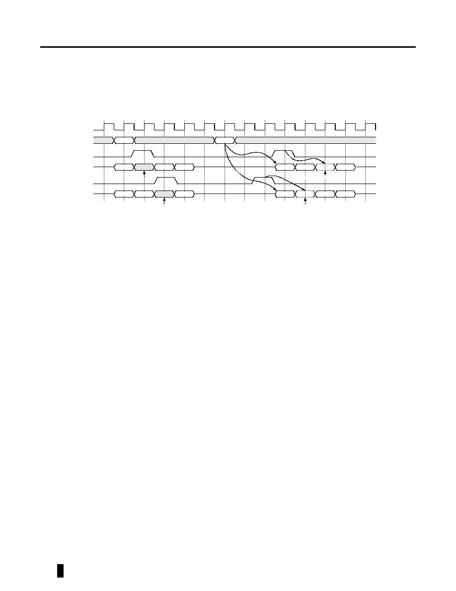
[Write Interrupted by Write]
Burst write operation can be interrupted by new write of the same or
the other bank. Random column access is allowed. WRITE to
WRITE interval is minimum 1 CLK.
[Write Interrupted by Read]
Burst write operation can be interrupted by read of the same or the
other bank. Random column access is allowed. WRITE to READ
interval is minimum 1 CLK. The input data on DQ at the interrupt-
ing READ cycle is "don't care". Using the DQMU / DQML to
prevent the bus contention is optional.
CLK
Command
A[9:0]
A[10]
BA
DQ
Figure 13. WRITE Interrupted by WRITE (BL=4)
Dj1
Dj0
Di0
Dk0
WRIT
Dk2
Dk1
Dl1
Dl0
Yi
Yk
Yl
Yj
0
0
0
0
0
1
0
0
Dl2
Dl3
WRIT
WRITE
WRITE
CLK
Command
DQ
Figure 14. WRITE interrupted by READ (BL=4, CL=3)
A[9:0]
A[10]
BA
DQMU,
WRITE
READ
0
0
Di0
Qj1
Qj0
Dk0
Dk1
WRITE
READ
Yi
Yj
Yk
Yl
0
0
0
0
0
1
Ql0

17
G-LINK Technology
May. 2003 (Rev.2.4)
[Write Interrupted by Precharge]
Burst write operation can be interrupted by precharge of the same
bank. Random column access is allowed. Because the write recov-
ery time (t
RDL
) is required between the last input data and the next
PRE, 3rd data should be masked with DQMU / DQML shown as
below.
[Write Interrupted by Burst Terminate]
Burst terminate command can terminate burst write operation. In
this case, the write recovery time is not required and the bank
remains active. The figure below shows the case 3 words of data are
written. Random column access is allowed. WRITE to TBST inter-
val is minimum 1 CLK.
CLK
Command
DQ
Figure 15. WRITE Interrupted by Precharge (BL=4)
A[9:0]
A[10]
BA
DQMU,
This data should be masked to satisfy t
RDL
requirement.
0
0
Di0
Ya
Xb
WRITE
PRE
ACT
0
Xb
0
0
Di1
CLK
Command
DQ
Figure 16. WRITE Interrupted by Burst Terminate (BL=4)
A[9:0]
A[10]
BA
DQMU,
Da0
Ya
WRITE
TBST
Da1
0
0
Da2

18
G-LINK Technology
May. 2003 (Rev. 2.4)
Auto Refresh
Single cycle of auto-refresh is initiated with a REFA (CS = RAS =
CAS = L, WE = CKE = H) command. The refresh address is gener-
ated internally. 4096 REFA cycles within 64 ms refresh 16 Mbit
memory cells. The auto-refresh is performed on each bank alter-
nately (ping-pong refresh). Before performing an auto-refresh, both
banks must be in the idle state. Additional commands must not be
supplied to the device before t
RC
from the REFA command.
Self Refresh
Self-refresh mode is entered by issuing a REFS command (CS =
RAS = CAS = L, WE = H, CKE = L). Once the self-refresh is initi-
ated, it is maintained as long as CKE is kept low. During the self-
refresh mode, CKE is asynchronous and the only enabled input (but
asynchronous), all other inputs including CLK are disabled and
ignored, and power consumption due to synchronous inputs is
saved. To exit the self-refresh, supplying stable CLK inputs, assert-
ing DESEL or NOP command and then asserting CKE (REFSX).
After t
RC
from REFSX both banks are in the idle state and a new
command can be issued after t
RC
, but DESEL or NOP commands
must be asserted till then.
CLK
CS
A[10:0]
Figure 17. Auto Refresh
RAS
CAS
WE
CKE
BA
NOP or Deselect
Minimum t
RC
Auto Refresh on Bank 0
Auto Refresh on Bank 1
minimum t
RC
for recovery
CLK
CS
A[10:0]
Figure 18. Self-Refresh
RAS
CAS
WE
CKE
BA
Stable CLK
Self Refresh Entry
Self Refresh Exit
NOP
new command
X
0

19
G-LINK Technology
May. 2003 (Rev.2.4)
CLK Suspend
CKE controls the internal CLK at the following cycle. Figure 19
and Figure 20 show how CKE works. By negating CKE, the next
internal CLK is suspended. The purpose of CLK suspend is power
down, output suspend or input suspend. CKE is a synchronous input
except during the self-refresh mode. CLK suspend can be per-
formed either when the banks are active or idle, but a command at
the following cycle is ignored.
ext. CLK
CKE
int. CLK
CLK
CKE
Figure 19. Power Down by CKE
Command
CKE
Command
Standby Power Down
Active Power Down
NOP
PRE
NOP
NOP
NOP
NOP
NOP
NOP
NOP
ACT
NOP
NOP
NOP
NOP
NOP
NOP
CLK
CKE
Figure 20. DQ Suspend by CKE
Command
DQ
WRITE
REA
D0
D1
D2
D3
Q0
Q1
Q2
Q3
20
G-LINK Technology
May. 2003 (Rev. 2.4)
DQMU / DQML Control
DQMU / DQML is a dual function signal defined as the data mask
for writes and the output disable for reads. During writes, DQMU /
DQML masks upper / lower input data word by word. DQMU /
DQML to write mask latency is 0. During reads, DQMU / DQML
forces upper / lower output to Hi-Z word by word. DQMU / DQML
to output Hi-Z latency is 2.
CLK
Command
Figure 21. DQMU / DQML Function
DQ[7:0]
DQMU
DQ[15:8]
DQML
Masked by DQML =
Masked by DQMU =
Disabled by DQMU
Disabled by DQML =
D2
D0
D3
Q0
Q1
Q3
WRITE
REA
D1
D0
D3
Q0
Q3
Q2

21
G-LINK Technology
May. 2003 (Rev.2.4)
E
LECTRICAL
S
PECIFICATIONS
Absolute Maximum Ratings
[1]
1. Stresses greater than those listed under "Absolute Maximum Ratings" may cause permanent damage to the device. This is a stress rating only, and functional operation
of the device at these or any other conditions above those indicated in the operational sections of this specification is not implied. Exposure to absolute maximum rating
conditions for extended periods may affect reliability.
Symbol
Parameter
Conditions
Ratings
Unit
V
DD
Supply Voltage
with respect to V
SS
-1.0 to 4.6
V
V
DDQ
Supply Voltage for Output
with respect to V
SSQ
-1.0 to 4.6
V
V
I
Input Voltage
with respect to V
SS
-1.0 to 4.6
V
V
O
Output Voltage
with respect to V
SSQ
-1.0 to 4.6
V
I
O
Output Current
50
mA
P
D
Power Dissipation
T
A
= 25 ∞C
1000
mW
T
OPR
Operating Temperature
comsumer
0 to 70
∞C
Industrial
-40 to 85
∞C
T
STG
Storage Temperature
-65 to 150
∞C
Recommended Operating Conditions (T
A
= 0 to +70∞C, unless otherwise noted)
Symbol
Parameter
Min
Typ
Max
Unit
V
DD
Supply Voltage
3.0
3.3
3.6
V
V
DDQ
Supply Voltage for Output
3.0
3.3
3.6
V
V
IH
[1]
High-Level Input Voltage all inputs
2.0
V
DDQ
+ 0.3
V
V
IL
[2]
Low-Level Input Voltage all inputs
-0.3
0.8
V
1. V
IH
(max) = 5.6 V for pulse width less than 3 ns.
2. V
IL
(min) = -2.0 V for pulse width less than 3 ns.
DC Characteristics (T
A
= 0 to +70∞C, V
DD
= V
DDQ
= 3.3 ±0.3V, V
SS
= V
SSQ
= 0 V, unless otherwise noted)
Symbol
Parameter
Test Conditions
Min
Max
Unit
V
OH
High-Level Output Voltage
I
OH
= -2 mA
2.4
V
V
OL
Low-Level Output Voltage
I
OL
= 2 mA
0.4
V
I
OZ
Off-state Output Current
Q floating V
O
= 0 to V
DDQ
-10
10
µA
I
I
Input Current
V
IH
= 0 to V
DDQ
+ 0.3 V
-10
10
µA
Capacitance (T
A
= 0 to +70∞C, V
DD
= V
DDQ
= 3.3 ±0.3 V, V
SS
= V
SSQ
= 0 V, unless otherwise noted)
Symbol
Parameter
Test Condition
Min
Max
Unit
C
I(A)
Input Capacitance, address pin
V
I
= V
SS
f = 1 MHz
V
I
= 25 mVrms
2.5
5
pF
C
I(C)
Input Capacitance, control pin
2.5
5
pF
C
I(K)
Input Capacitance, CLK pin
2.5
5
pF
C
I/O
Input Capacitance, I/O pin
4
7
pF
22
G-LINK Technology
May. 2003 (Rev. 2.4)
Average Supply Current from V
DD
(T
A
= 0 to +70∞C, V
DD
= V
DDQ
= 3.3 ±0.3 V, V
SS
= V
SSQ
= 0 V, unless otherwise noted)
Symbol
Parameter
Test Conditions
Rating (Max)
Unit
-6
-7
-8
-10
I
CC1S
Operating Current, Single Bank
t
RC
= min, t
CLK
= min, BL = 1, CL = 3
120
110
100
90
mA
I
CC1D
Operating Current, Dual Bank
t
RC
= min, t
CLK
= min, BL = 1, CL = 3
170
150
140
120
mA
I
CC2H
Standby Current, CKE = H
both banks idle, t
CLK
= min, CKE = H
20
20
20
20
mA
I
CC2L
Standby Current, CKE = L
both banks idle, t
CLK
= min, CKE = L
2
2
2
2
mA
I
CC3H
Active Standby Current, CKE = H
both banks active, t
CLK
= min, CKE = H
35
35
35
35
mA
I
CC3L
Active Standby Current, CKE = L
both banks active, t
CLK
= min, CKE = L
4
4
4
4
mA
I
CC4
Burst Current
t
CLK
= min, BL = 4, CL = 3, both banks
active
180
170
160
140
mA
I
CC5
Auto-Refresh Current
t
RC
= min, t
CLK
= min
110
100
90
80
mA
I
CC6
Self-Refresh Current
CKE < 0.2 V
1
1
1
1
mA
Low Power
500
500
500
500
µA
AC Characteristics (T
A
= 0 to +70∞C, V
DD
= V
DDQ
= 3.3 ±0.3 V, V
SS
= V
SSQ
= 0 V, unless otherwise noted)
[1]
Symbol
Parameter
-6
-7
-8
-10
Unit
Min
Max
Min
Max
Min
Max
Min
Max
t
CLK
CLK Cycle Time
CL=2
-
9
10
13
ns
CL=3
6
7
8
10
ns
t
CH
CLK High Pulse Width
2.5
3
3
3.5
ns
t
CL
CLK Low Pulse Width
2.5
3
3
3.5
ns
t
T
Transition Time of CLK
1
10
1
10
1
10
1
10
ns
t
IS
Input Setup Time (all inputs)
2
2.5
2.5
2.5
ns
t
IH
Input Hold Time (all inputs)
1
1
1
1
ns
t
RC
Row Cycle Time
60
63
72
90
ns
t
RCD
Row to Column Delay
18
21
24
30
ns
t
RAS
Row Active Time
42
100k
42
100k
48
100k
60
100k
ns
t
RP
Row Precharge Time
18
21
24
30
ns
t
CCD
Column Address to Column Adress Delay
1
1
1
1
CLK
t
RRD
Act to Act Delay Time
2
2
2
2
CLK
t
RSC
Mode Register Set Cycle Time
1
1
1
1
CLK
t
RDL
Last Data-In to Row Precharge Delay
1
1
1
1
CLK
t
REF
Refresh Interval Time
65.6
65.6
65.6
65.6
ms
1. Input Pulse Levels: 0.4 V to 2.4 V with t
r
/t
f
= +1/+1 ns. Input Timing Measurement Level: 1.4 V.
1.4
CLK
Signal
1.4
Any AC timing is
referenced to the
input signal crossing

23
G-LINK Technology
May. 2003 (Rev.2.4)
Switching Characteristics (T
A
= 0 to +70∞C, V
DD
= V
DDQ
= 3.3 ±0.3 V, V
SS
= V
SSQ
= 0 V unless otherwise
noted)
Symbol
Parameter
-6
-7
-8
-10
Unit
Min
Max
Min
Max
Min
Max
Min
Max
t
AC
Access Time from
CL=2
-
7
9
10
ns
CL=3
5.5
6
6
7
ns
t
OH
Output Hold Time from CLK
2.5
2.5
3
3
ns
t
OLZ
Delay Time, Output Low Impedance from
CLK
1
1
1
1
ns
t
OHZ
Delay Time, Output High Imped-
ance from CLK
CL=2
-
7
7
9
ns
CL=3
5.5
6
6
7
ns
1.4
CLK
DQ
1.4
Output Timing Measurement Reference Point
1.4
CLK
DQ
1.4
t
AC
t
OH
-
+
V
REF
=
V
TT
= 1.4V
V
OUT
50
50 pF
(1)
Figure 22. Output Load Condition
1. For GLT5160L16-6/7, the Output Load is 30
t
OHZ
t
OLZ

24
G-LINK Technology
May. 2003 (Rev. 2.4)
Figure 23. WRITE Cycle (single bank) BL=4
t
RCD
t
RDL
t
RAS
t
RP
t
RC
Xa
HIG
Xb
Xb
Xa
Di0
Di1
Di2
Di3
CLK
CS
RAS
CAS
WE
CKE
DQMU,
A[9:0]
A[10]
BA
DQ
ACT
B0
B0
B0
B0
WRITE
PRE
ACT
Yi

25
G-LINK Technology
May. 2003 (Rev.2.4)
Figure 24. WRITE Cycle (Dual Bank) BL=4
t
RCD
t
RDL
t
RAS
Xa
Xa
Yb
Ya
Xb
Xb
Da0
Da1
Da2
Da3
Db0
Db1
Db2
Db3
t
RCD
t
RRD
t
RAS
t
RDL
CLK
CS
RAS
CAS
WE
CKE
DQMU,
A[9:0]
A[10]
BA
DQ
HIG
ACT
B0
B0
B
B1
B0
B1
WRIT
WRIT
ACT
PRE
PRE

26
G-LINK Technology
May. 2003 (Rev. 2.4)
Figure 25. READ Cycle (Single Bank) BL=4, CL=3
t
RCD
t
RAS
t
RC
Xa
Xa
Xb
Ya
t
RP
Xb
CLK
CS
RAS
CAS
WE
CKE
DQMU,
A[9:0]
A[10]
BA
DQ
Qa0
Qa1
Qa2
Qa3
ACT
READ
PRE
B0
ACT
B0

27
G-LINK Technology
May. 2003 (Rev.2.4)
Figure 26. READ Cycle (Dual Bank) BL=4, CL=3
t
RCD
Xa
Yb
Ya
Xb
Xa
Xb
Xc
Xc
t
RCD
t
RRD
t
RC
t
RAS
t
RAS
t
RP
CLK
CS
RAS
CAS
WE
CKE
DQMU,
A[9:0]
A[10]
BA
DQ
Qa0
Qa1
Qa2
Qa3
Qb0
Qb1
Qb2
Qb3
ACT
READ
READ
PRE
ACT
PRE
ACT

28
G-LINK Technology
May. 2003 (Rev. 2.4)
CLK
CS
RAS
CAS
WE
CKE
DQMU,
A[9:0]
A[10]
BA
DQ
Figure 27. WRITE to READ (Single Bank) BL=4, CL=3
Xa
Yb
Ya
Xa
t
RAS
t
RCD
Da0
Da1
Da2
Da3
Qb0
Qb1
Qb2
Qb3
ACT
WRITE
READ
PRE

29
G-LINK Technology
May. 2003 (Rev.2.4)
CLK
CS
RAS
CAS
WE
CKE
DQMU,
A[9:0]
A[10]
BA
DQ
Figure 28. WRITE to READ (Dual Bank) BL=4, CL=3
Xa
Yb
Ya
Xb
Xc
Xa
Xb
Xc
t
RCD
t
RRD
t
RC
t
RAS
t
RAS
t
RP
t
WR
t
RCD
Da0
Da1
Da2
Da3
Qb0
Qb1
Qb2
Qb3
ACT
WRITE
ACT
REA
PRE
PRE
ACT

30
G-LINK Technology
May. 2003 (Rev. 2.4)
CLK
CS
RAS
CAS
WE
CKE
DQML
A[9:0]
A[10]
BA
DQ[7:0]
Figure 29. DQM Byte Control for WRITE to READ (Single Bank) BL=4, CL=3
DQMU
DQ[15:8]
Xa
Yb
Ya
Xa
Qb3
t
RAS
t
RCD
Da0
Da2
Da3
Da0
Da3
Qb0
Qb1
Qb2
Qb0
Qb1
ACT
WRITE
READ
PRE
Da1
31
G-LINK Technology
May. 2003 (Rev.2.4)
CLK
CS
RAS
CAS
WE
CKE
DQMU,
A[9:0]
A[10]
BA
DQ
Figure 30. READ to WRITE (Single Bank) BL=4, CL=3
Xa
Yb
Ya
Xa
t
RAS
t
RCD
t
RDL
for output disable
Db0
Db2
Db3
Qa0
Qa1
Db1
READ
PRE
WRITE
PRE
32
G-LINK Technology
May. 2003 (Rev. 2.4)
CLK
CS
RAS
CAS
WE
CKE
DQMU,
A[9:0]
A[10]
BA
DQ
Figure 31. READ to WRITE (Dual Bank) BL=4, CL=3
for output disable
Xa
Yb
Ya
Xb
Xa
Xb
Xc
Xc
t
RC
t
RCD
t
RRD
t
RAS
t
RAS
t
RP
t
RCD
t
RDL
Db1
Db3
Qa0
Qa1
Db2
ACT
READ
PRE
ACT
ACT
WRITE
PRE
Db0

33
G-LINK Technology
May. 2003 (Rev.2.4)
CLK
CS
RAS
CAS
WE
CKE
A[9:0]
A[10]
BA
DQ
Figure 32. Write with Auto-Precharge BL=4
DQMU,
Xa
Xb
Ya
Xa
Xb
t
RC
t
RCD
t
RDL
+ t
RP
Internal Precharge starts
this timing depends on BL
Da0
Da1
Da2
Da3
ACT
WRITE
ACT
34
G-LINK Technology
May. 2003 (Rev. 2.4)
CLK
CS
RAS
CAS
WE
CKE
A[9:0]
A[10]
BA
DQ
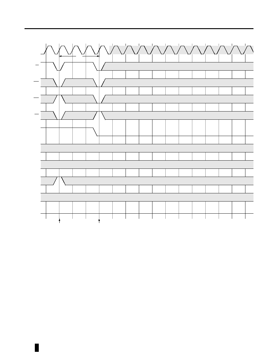
Figure 33. Read with Auto-Precharge BL=4, CL=3
DQMU,
Xa
Xb
Ya
Xa
Xb
Internal Precharge start s @ CL=3, BL=4
this timing depends on CL and BL
t
RC
t
RCD
t
RP
Qa0
Qa1
Qa2
Qa3
ACT
READ
ACT

35
G-LINK Technology
May. 2003 (Rev.2.4)
CLK
CS
RAS
CAS
WE
CKE
A[9:0]
A[10]
BA
DQ
Figure 34. Auto-Refresh
DQMU,
If any bank is active, it
must be precharged
t
RC
t
RP
PRE
REF S
REF
DC High
36
G-LINK Technology
May. 2003 (Rev. 2.4)
CLK
CS
RAS
CAS
WE
CKE
A[9:0]
A[10]
BA
DQ
Figure 35. Self-Refresh Entry
DQMU,
If any bank is active, it
must be precharged
t
RP
PRE
REF S

37
G-LINK Technology
May. 2003 (Rev.2.4)
CLK
CS
RAS
CAS
WE
CKE
A[9:0]
A[10]
BA
DQ
Figure 36. Self-Refresh Exit
DQMU,
Xa
Xa
NOP or desel
t
RC
t
SRX
Internal CLK Re-start
ACT

38
G-LINK Technology
May. 2003 (Rev. 2.4)
CLK
CS
RAS
CAS
WE
CKE
A[9:0]
A[10]
BA
DQ
Figure 37. Mode Register Set BL=4, CL=3
DQMU,
Xa
Ya
Mode
Xa
t
RP
t
RSC
t
RCD
If any bank is
active, it must be
precharged
Qa0
Qa1
Qa2
PRE
MRS
ACT
READ

39
G-LINK Technology
May. 2003 (Rev.2.4)
P
ACKAGING
I
NFORMATION
Figure 38. 50-Pin 400 mil TSOP II Pin Assignment
V
DD
DQ0
V
SSQ
DQ2
DQ3
V
DDQ
DQ4
DQ5
V
SSQ
DQ6
DQML
WE
CAS
RAS
CS
BA
A10
V
DDQ
DQ11
DQ10
V
SSQ
DQ9
DQ8
V
DDQ
NC
DQMU
CLK
A9
A8
A7
A6
A5
A4
V
SS
1
2
3
4
5
6
7
8
9
10
13
14
15
16
17
18
19
20
44
43
42
41
40
39
38
37
36
35
32
31
30
29
28
27
26
Top View
A0
A1
21
22
DQ7
V
DDQ
11
12
34
33
CKE
NC
23
24
25
45
46
47
48
49
50
A2
A3
V
DD
DQ12
DQ13
V
SSQ
DQ14
DQ15
V
SS
DQ1
A
B
C
D
E
F
G
H
J
K
L
M
N
P
R
6
5
7
4
3
2
1
VSS
DQ14
DQ13
DQ12
DQ10
DQ9
DQ8
NC
NC
NC
CKE
A11
A8
A6
VSS
VSSQ
DQ15
VSSQ
VDDQ
DQ11
VSSQ
VDDQ
NC
NC
UDQM
CLK
NC
A9
A7
A5
A4
DQ0
VDDQ
VSSQ
DQ4
VDDQ
NC
NC
LDQM
RAS#
NC
NC
A0
A2
A3
VDD
DQ1
DQ2
DQ3
DQ5
DQ6
DQ7
NC
WE#
CAS#
CS#
NC
A10
A1
VDD
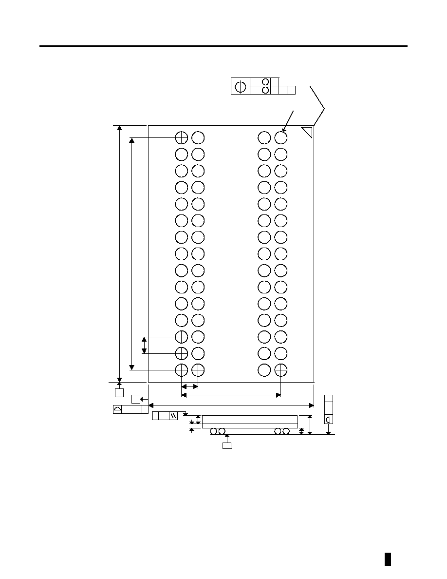
Figure 38-1. 60-Ball VFBGA Ball

40
G-LINK Technology
May. 2003 (Rev. 2.4)
Figure 39. 50-Pin 400 mil Plastic TSOP II Package Dimensions
21.35max.
20.95±0.1
0.125±0.075
Detail A
0.5±0.1
Detail A
0.3+0.1/-0.05
0.8
1.0±0.10
0.125
+0.05
-0.02
10.6±0.1
0
0
~10
0
26
1
0.1
25
50
41
G-LINK Technology
May. 2003 (Rev.2.4)
A
B
C
D
E
F
G
H
J
K
L
M
N
P
R
2
3
1
4
5
6
7
0.65
3.90
6.40 ± 0.10
0.65
9.10
0.45 ± 0.03
0.27 ± 0.05
1.00 MAX
0.20
C
SEATING PLANE
C
0.20
C
0.15(4X) C
B
A
0.35~0.40(60X)
0.08
0.15
M
M
C
C
A
B
A1 CORNER
0.21 ± 0.04
10.10 ± 0.10
60-Ball VFBGA ( BOTTOM VIEW )

42
G-LINK Technology
May. 2003 (Rev. 2.4)
O
RDERING
I
NFO
GLT5160L16
Part Number
Mode
Cycle Time
Max Frequency
Interface
Package
GLT5160L16-10TC
Synchronous
10
100 MHz
LVTTL
50-Pin 400 mil Plastic TSOP II
GLT5160L16-8TC
Synchronous
8
125 MHz
LVTTL
50-Pin 400 mil Plastic TSOP II
GLT5160L16-7TC
Synchronous
7
143 MHz
LVTTL
50-Pin 400 mil Plastic TSOP II
GLT5160L16-6TC
Synchronous
6
166 MHz
LVTTL
50-Pin 400 mil Plastic TSOP II
GLT5160L16-10FJ
Synchronous
10
100 MHz
LVTTL
60-Ball VFBGA
GLT5160L16-8FJ
Synchronous
8
125 MHz
LVTTL
60-Ball VFBGA
GLT5160L16-7FJ
Synchronous
7
143 MHz
LVTTL
60-Ball VFBGA
GLT5160L16-6FJ
Synchronous
6
166 MHz
LVTTL
60-Ball VFBGA
GLT5160L16I-10TC
Synchronous
10
100 MHz
LVTTL
50-Pin 400 mil Plastic TSOP II
GLT5160L16I-8TC
Synchronous
8
125 MHz
LVTTL
50-Pin 400 mil Plastic TSOP II
GLT5160L16I-7TC
Synchronous
7
143 MHz
LVTTL
50-Pin 400 mil Plastic TSOP II
GLT5160L16I-6TC
Synchronous
6
166 MHz
LVTTL
50-Pin 400 mil Plastic TSOP II
GLT5160L16I-10FJ
Synchronous
10
100 MHz
LVTTL
60-Ball VFBGA
GLT5160L16I-8FJ
Synchronous
8
125 MHz
LVTTL
60-Ball VFBGA
GLT5160L16I-7FJ
Synchronous
7
143 MHz
LVTTL
60-Ball VFBGA
GLT5160L16I-6FJ
Synchronous
6
166 MHz
LVTTL
60-Ball VFBGA
GLT5160L16P-10TC
Synchronous
10
100 MHz
LVTTL
50-Pin 400 mil Plastic TSOP II
GLT5160L16P-8TC
Synchronous
8
125 MHz
LVTTL
50-Pin 400 mil Plastic TSOP II
GLT5160L16P-7TC
Synchronous
7
143 MHz
LVTTL
50-Pin 400 mil Plastic TSOP II
GLT5160L16P-6TC
Synchronous
6
166 MHz
LVTTL
50-Pin 400 mil Plastic TSOP II
GLT5160L16P-10FJ
Synchronous
10
100 MHz
LVTTL
60-Ball VFBGA
GLT5160L16P-8FJ
Synchronous
8
125 MHz
LVTTL
60-Ball VFBGA
GLT5160L16P-7FJ
Synchronous
7
143 MHz
LVTTL
60-Ball VFBGA
GLT5160L16P-6FJ
Synchronous
6
166 MHz
LVTTL
60-Ball VFBGA

43
G-LINK Technology
May. 2003 (Rev.2.4)
Parts Numbers (Top Mark) Definition for SDRAM and SGRAM :
GLT 5 160 L 16 - 7 TC
5 : Synchronous
DRAM
9 : SGRAM
DENSITY
40 : 4M
160 : 16M
320 : 32M,4Bank
640 : 64M
1280 : 128M
VOLTAGE
Blank : 5V
L : 3.3V
M : 2.5V
N : 2.0V
CONFIG.
04 : x04
08 : x08
16 : x16
32 : x32
SPEED
SDRAM :
5 : 5ns/200 MHZ
5.5 : 5.5ns/183 MHZ
6 : 6ns/166 MHZ
7 : 7ns/143 MHZ
8 : 8ns/125 MHZ
10 : 10ns/100 MHZ
PACKAGE
TS : TSOP(Type I)
ST : sTSOP(Type I)
TC : TSOPll
TQ : TQFP
FJ : 60Ball VFBGA
Temperature Range
E : Extended Temperature
I : Industrial Temperature
Blank : Commercial Temperature
Environmental Option
P : Pb≠free part
POWER
Blank : Standard
L : Low Power
LL : Low Low Power

© 1998 G-LINK Technology
All rights reserved. No part of this document may be copied or reproduced in any form or by any means or transferred to any third party without the prior written consent of G-LINK Technology.
Circuit diagrams utilizing G-LINK products are included as a means of illustrating typical semiconductor applications. Complete information sufficient for design purposes is not necessarily given.
G-LINK Technology reserves the right to change products or specifications without notice.
The information contained in this document does not convey any license under copyrights, patent rights or trademarks claimed and owned by G-LINK or its subsidiaries. G-LINK assumes no liability for
G-LINK applications assistance, customer's product design, or infringement of patents arising from use of semiconductor devices in such systems' designs. Nor does G-LINK warrant or represent that any
patent right, copyright, or other intellectual property right of G-LINK covering or relating to any combination, machine, or process in which such semiconductor devices might be or are used.
G-LINK Technology's products are not authorized for use in life support devices or systems. Life support devices or systems are device or systems which are: a) intended for surgical implant into the human
body and b) designed to support or sustain life; and when properly used according to label instructions, can reasonably be expected to cause significant injury to the user in the event of failure.
The information contained in this document is believed to be entirely accurate. However, G-LINK Technology assumes no responsibility for inaccuracies.
G-LINK Technology Corporation, Taiwan
www.glink.com.tw
sales@glink.com.tw
TEL: 886-2-2659-9658